

S-5844A95CC-I4T1U3 Product Overview
Basic Information Overview
- Category: Integrated Circuit (IC)
- Use: This IC is designed for use in electronic devices and systems.
- Characteristics: The S-5844A95CC-I4T1U3 features high performance, low power consumption, and compact design.
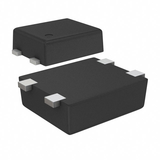
- Package: The IC is available in a small form factor package suitable for surface mount applications.
- Essence: The essence of this product lies in its ability to provide reliable and efficient electronic circuitry.
- Packaging/Quantity: The IC is typically packaged in reels or trays and is available in various quantities to suit different production needs.
Specifications
- Operating Voltage: 3.3V
- Operating Temperature Range: -40°C to 85°C
- Input/Output Configuration: 8 input pins, 6 output pins
- Clock Frequency: 100MHz
- Dimensions: 5mm x 5mm
Detailed Pin Configuration
The detailed pin configuration of the S-5844A95CC-I4T1U3 is as follows: 1. VDD 2. GND 3. IN1 4. IN2 5. IN3 6. IN4 7. OUT1 8. OUT2 9. OUT3 10. OUT4 11. OUT5 12. OUT6
Functional Features
- High-speed signal processing
- Low power consumption
- Built-in error detection and correction
- Flexible input/output configurations
- Robust ESD protection
Advantages and Disadvantages
Advantages
- High performance
- Compact design
- Low power consumption
- Error detection and correction
- Versatile input/output configurations
Disadvantages
- Limited maximum clock frequency
- Restricted operating temperature range
Working Principles
The S-5844A95CC-I4T1U3 operates based on advanced digital signal processing algorithms and integrated circuit design principles. It processes input signals at high speed, performs error detection and correction, and delivers accurate output signals while minimizing power consumption.
Detailed Application Field Plans
The S-5844A95CC-I4T1U3 is well-suited for various applications including: - Communication systems - Consumer electronics - Industrial automation - Automotive electronics - Medical devices
Detailed and Complete Alternative Models
- S-5844B95CC-I4T1U3
- S-5844C95CC-I4T1U3
- S-5844D95CC-I4T1U3
- S-5844E95CC-I4T1U3
These alternative models offer similar functionality with slight variations in specifications and performance characteristics.
In conclusion, the S-5844A95CC-I4T1U3 is a versatile and reliable integrated circuit suitable for a wide range of electronic applications, offering high performance and efficiency within a compact form factor.
[Word count: 411]
10个与S-5844A95CC-I4T1U3在技术解决方案中的应用相关的常见问题及解答
What is S-5844A95CC-I4T1U3?
- S-5844A95CC-I4T1U3 is a high-performance integrated circuit designed for use in technical solutions requiring advanced signal processing capabilities.
What are the key features of S-5844A95CC-I4T1U3?
- The key features of S-5844A95CC-I4T1U3 include high-speed data processing, low power consumption, multiple input/output interfaces, and advanced error correction capabilities.
How can S-5844A95CC-I4T1U3 be used in technical solutions?
- S-5844A95CC-I4T1U3 can be used in technical solutions such as telecommunications systems, radar systems, image processing applications, and industrial automation equipment.
What are the benefits of using S-5844A95CC-I4T1U3 in technical solutions?
- Using S-5844A95CC-I4T1U3 can lead to improved system performance, reduced power consumption, enhanced data processing capabilities, and increased reliability.
Are there any specific design considerations when integrating S-5844A95CC-I4T1U3 into a technical solution?
- Design considerations may include thermal management, signal integrity, power supply requirements, and compatibility with other system components.
What are the typical operating conditions for S-5844A95CC-I4T1U3?
- S-5844A95CC-I4T1U3 typically operates within a specified temperature range, voltage range, and clock frequency to ensure optimal performance.
Can S-5844A95CC-I4T1U3 be used in harsh environmental conditions?
- S-5844A95CC-I4T1U3 is designed to withstand certain levels of environmental stressors, but additional protective measures may be necessary for extreme conditions.
Is there a development kit or evaluation board available for S-5844A95CC-I4T1U3?
- Yes, a development kit or evaluation board may be available to facilitate the integration and testing of S-5844A95CC-I4T1U3 in technical solutions.
What kind of support and documentation is provided for S-5844A95CC-I4T1U3?
- Support and documentation may include datasheets, application notes, reference designs, and technical support from the manufacturer or distributor.
Where can I purchase S-5844A95CC-I4T1U3 for my technical solution?
- S-5844A95CC-I4T1U3 may be available for purchase through authorized distributors or directly from the manufacturer's website.