

AD667JNZ
Product Overview
Category
AD667JNZ belongs to the category of integrated circuits (ICs).
Use
The AD667JNZ is primarily used for analog-to-digital conversion in various electronic systems.
Characteristics
- High-speed and high-resolution analog-to-digital conversion
- Low power consumption
- Wide input voltage range
- Small form factor
Package
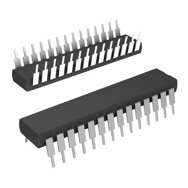
The AD667JNZ comes in a standard 28-pin plastic dual inline package (PDIP).
Essence
The essence of the AD667JNZ lies in its ability to accurately convert analog signals into digital data, enabling further processing and analysis.
Packaging/Quantity
The AD667JNZ is typically packaged in reels or tubes, with a quantity of 25 units per package.
Specifications
- Resolution: 12 bits
- Sampling Rate: Up to 1 MSPS (Million Samples Per Second)
- Input Voltage Range: ±10V
- Power Supply: +5V
- Operating Temperature Range: -40°C to +85°C
Detailed Pin Configuration
The AD667JNZ has a total of 28 pins. The pin configuration is as follows:
- VREF-
- VREF+
- AGND
- VIN-
- VIN+
- DGND
- D0
- D1
- D2
- D3
- D4
- D5
- D6
- D7
- D8
- D9
- D10
- D11
- CS
- RD
- WR
- A0
- A1
- A2
- A3
- A4
- A5
- VDD
Functional Features
- High-speed successive approximation analog-to-digital conversion
- On-chip sample-and-hold circuitry for accurate signal acquisition
- Parallel output interface for easy integration with microcontrollers or digital systems
- Built-in reference voltage generation for simplified system design
Advantages and Disadvantages
Advantages
- High resolution and accuracy in analog-to-digital conversion
- Fast sampling rate enables real-time data acquisition
- Low power consumption for energy-efficient applications
- Compact package size allows for space-saving designs
Disadvantages
- Limited input voltage range compared to some other models
- Requires an external power supply (+5V) for operation
Working Principles
The AD667JNZ utilizes a successive approximation technique to convert analog signals into digital data. It employs a sample-and-hold circuit to capture the input voltage, which is then processed by an internal ADC core. The converted digital data is made available through the parallel output interface.
Detailed Application Field Plans
The AD667JNZ finds applications in various fields, including:
- Industrial automation: Used for precise measurement and control of analog signals in manufacturing processes.
- Medical devices: Enables accurate digitization of physiological signals for diagnostic purposes.
- Communications: Used in data acquisition systems for signal processing and analysis.
- Test and measurement equipment: Provides high-resolution measurements for scientific research and engineering applications.
Detailed and Complete Alternative Models
- AD7685: 16-bit, 250 kSPS SAR ADC
- ADS8860: 18-bit, 1 MSPS SAR ADC
- MAX11131: 12-bit, 500 kSPS SAR ADC
- LTC1867: 16-bit, 250 kSPS SAR ADC
These alternative models offer different resolutions, sampling rates, and features to suit specific application requirements.
In conclusion, the AD667JNZ is a high-speed and high-resolution analog-to-digital converter that finds applications in various fields. Its compact size, low power consumption, and accurate conversion make it a versatile choice for electronic systems requiring precise data acquisition.
Word count: 511
10个与AD667JNZ在技术解决方案中的应用相关的常见问题及解答
Sure! Here are 10 common questions and answers related to the application of AD667JNZ in technical solutions:
Q: What is AD667JNZ? A: AD667JNZ is a high-speed, low-power analog-to-digital converter (ADC) manufactured by Analog Devices.
Q: What is the resolution of AD667JNZ? A: AD667JNZ has a resolution of 12 bits, meaning it can represent analog signals with 4096 discrete levels.
Q: What is the maximum sampling rate of AD667JNZ? A: AD667JNZ can sample at a maximum rate of 100 megasamples per second (MSPS).
Q: What is the input voltage range of AD667JNZ? A: The input voltage range of AD667JNZ is typically ±5 volts.
Q: Does AD667JNZ require an external reference voltage? A: Yes, AD667JNZ requires an external reference voltage for accurate conversion. It supports both internal and external references.
Q: Can AD667JNZ be used in single-ended or differential mode? A: AD667JNZ can be used in both single-ended and differential mode, depending on the application requirements.
Q: What is the power supply voltage range for AD667JNZ? A: AD667JNZ operates from a single power supply voltage ranging from +4.75V to +5.25V.
Q: Does AD667JNZ have built-in digital signal processing (DSP) features? A: No, AD667JNZ is a standalone ADC and does not have built-in DSP features. It focuses on high-speed and high-resolution conversion.
Q: What is the typical power consumption of AD667JNZ? A: The typical power consumption of AD667JNZ is around 1.5 watts.
Q: What are some common applications of AD667JNZ? A: AD667JNZ is commonly used in applications such as communications, medical imaging, industrial automation, and scientific instrumentation where high-speed and high-resolution analog-to-digital conversion is required.
Please note that the answers provided here are general and may vary depending on specific datasheet specifications and application requirements.