

AD7233BNZ
Product Overview
Category
AD7233BNZ belongs to the category of integrated circuit (IC) chips.
Use
The AD7233BNZ is primarily used for digital-to-analog conversion (DAC) applications.
Characteristics
- High precision and accuracy in converting digital signals to analog outputs.
- Low power consumption.
- Compact size, suitable for integration into various electronic devices.
- Wide operating voltage range.
- Fast conversion speed.
Package
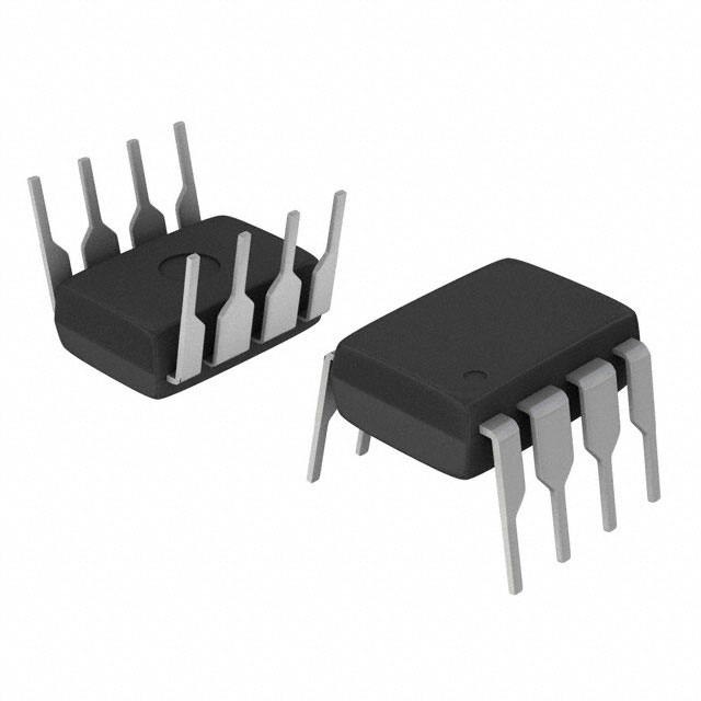
AD7233BNZ is available in a standard 24-pin plastic dual in-line package (PDIP).
Essence
The essence of AD7233BNZ lies in its ability to convert digital data into corresponding analog signals with high precision and efficiency.
Packaging/Quantity
AD7233BNZ is typically packaged in reels or tubes, with a quantity of 50 units per package.
Specifications
- Resolution: 12 bits
- Number of Channels: 4
- Supply Voltage Range: 2.7V to 5.5V
- Operating Temperature Range: -40°C to +85°C
- Output Voltage Range: 0V to VREF
- Conversion Time: 10µs (typical)
Detailed Pin Configuration
- VDD: Positive supply voltage
- VSS: Ground reference
- AGND: Analog ground
- REFOUT: Reference output voltage
- REFIN: Reference input voltage
- VREF: Reference voltage
- D0-D11: Digital input pins
- CS: Chip select input
- WR: Write control input
- RD: Read control input
- A0-A3: Address inputs
- DB0-DB7: Data bus pins
- OUTA: Analog output channel A
- OUTB: Analog output channel B
- OUTC: Analog output channel C
- OUTD: Analog output channel D
- AGND: Analog ground
- VSS: Ground reference
- VDD: Positive supply voltage
- NC: No connection
- NC: No connection
- NC: No connection
- NC: No connection
- NC: No connection
Functional Features
- High-resolution digital-to-analog conversion.
- Four independent analog output channels.
- Serial interface for easy integration with microcontrollers and other digital systems.
- Power-down mode for reduced power consumption during idle periods.
- Internal reference voltage generation.
Advantages and Disadvantages
Advantages
- High precision and accuracy in digital-to-analog conversion.
- Compact size allows for easy integration into various electronic devices.
- Wide operating voltage range enables compatibility with different power supplies.
- Fast conversion speed ensures real-time response.
Disadvantages
- Limited number of channels (4) compared to some alternative models.
- May require additional external components for certain applications.
Working Principles
AD7233BNZ operates by receiving digital input data and converting it into corresponding analog output voltages. The internal circuitry processes the digital signals and generates precise analog outputs based on the provided input values. The chip utilizes a combination of digital logic and analog circuitry to achieve accurate conversion.
Detailed Application Field Plans
AD7233BNZ finds applications in various fields, including but not limited to: 1. Audio equipment: Used for digital-to-analog conversion in audio amplifiers, mixers, and sound systems. 2. Instrumentation: Enables precise control of analog signals in measurement and testing equipment. 3. Industrial automation: Utilized in control systems for converting digital control signals into analog outputs. 4. Communication systems: Used for signal processing and modulation in telecommunication devices. 5. Automotive electronics: Enables digital-to-analog conversion in automotive audio systems and control modules.
Detailed and Complete Alternative Models
- AD5620: 12-bit, single-channel DAC with SPI interface.
- MCP4921: 12-bit, single-channel DAC with SPI interface.
- MAX5216: 16-bit, quad-channel DAC with I2C interface.
- LTC2631: 12-bit, dual-channel DAC with I2C interface.
- DAC8562: 16-bit, dual-channel DAC with SPI interface.
These alternative models offer similar functionality to AD7233BNZ and can be considered based on specific application requirements.
Word count: 550 words
10个与AD7233BNZ在技术解决方案中的应用相关的常见问题及解答
Sure! Here are 10 common questions and answers related to the application of AD7233BNZ in technical solutions:
Q: What is AD7233BNZ? A: AD7233BNZ is a digital-to-analog converter (DAC) chip manufactured by Analog Devices.
Q: What is the resolution of AD7233BNZ? A: AD7233BNZ has a resolution of 12 bits, allowing it to convert digital signals into analog voltages with high precision.
Q: What is the operating voltage range of AD7233BNZ? A: AD7233BNZ operates within a voltage range of +5V to +15V.
Q: Can AD7233BNZ be used for both single-ended and differential output applications? A: Yes, AD7233BNZ can be used for both single-ended and differential output applications.
Q: What is the maximum output current of AD7233BNZ? A: The maximum output current of AD7233BNZ is typically 2 mA.
Q: Does AD7233BNZ support multiple channels? A: Yes, AD7233BNZ supports dual-channel operation, allowing it to generate two independent analog outputs.
Q: What is the interface used to communicate with AD7233BNZ? A: AD7233BNZ uses a serial interface called SPI (Serial Peripheral Interface) for communication with microcontrollers or other devices.
Q: Can AD7233BNZ operate in both unipolar and bipolar modes? A: Yes, AD7233BNZ can operate in both unipolar (0V to Vref) and bipolar (-Vref/2 to +Vref/2) modes.
Q: What is the settling time of AD7233BNZ? A: The settling time of AD7233BNZ is typically 10 μs, ensuring fast and accurate voltage outputs.
Q: Is AD7233BNZ suitable for precision measurement applications? A: Yes, AD7233BNZ is suitable for precision measurement applications due to its high resolution and low integral nonlinearity (INL).
Please note that these answers are general and may vary depending on specific application requirements and datasheet specifications.