

AD7548JNZ
Product Overview
Category: Integrated Circuit (IC)
Use: The AD7548JNZ is a high-performance, 12-bit digital-to-analog converter (DAC) IC. It converts digital signals into analog voltages with exceptional accuracy and precision.
Characteristics: - Resolution: 12 bits - Number of Channels: 1 - Output Type: Voltage - Interface Type: Parallel - Supply Voltage: 5V - Operating Temperature Range: -40°C to +85°C
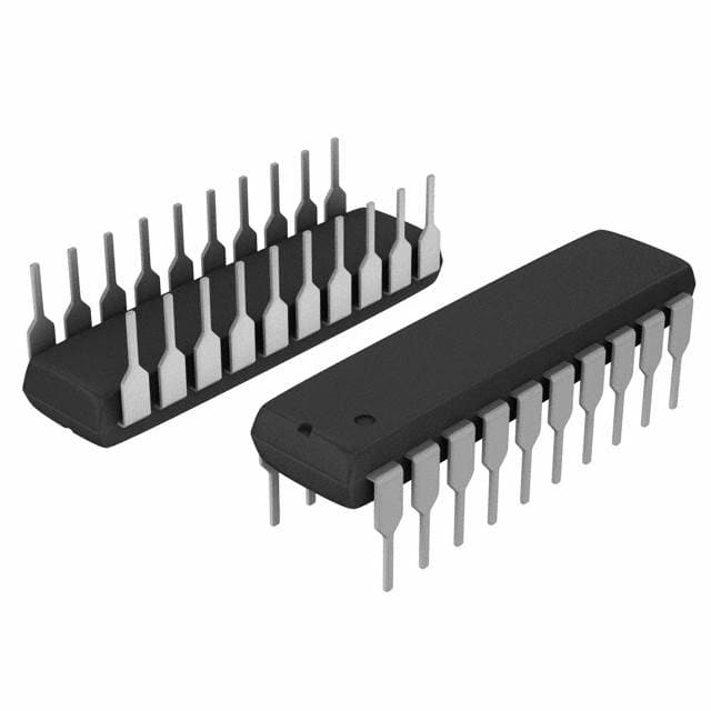
Package: The AD7548JNZ is available in a 20-pin PDIP (Plastic Dual In-line Package) format.
Essence: The essence of the AD7548JNZ lies in its ability to convert digital data into precise analog voltages, making it suitable for various applications that require accurate analog signal generation.
Packaging/Quantity: The AD7548JNZ is typically sold in reels or tubes containing multiple units. The exact quantity may vary depending on the supplier.
Specifications
- Resolution: 12 bits
- Reference Voltage Range: 0V to Vref
- Output Voltage Range: 0V to Vref
- Differential Non-Linearity (DNL): ±1 LSB (Least Significant Bit)
- Integral Non-Linearity (INL): ±2 LSB
- Settling Time: 10µs
- Power Supply Rejection Ratio (PSRR): 80dB
- Total Harmonic Distortion (THD): -70dB
- Spurious-Free Dynamic Range (SFDR): 75dB
Detailed Pin Configuration
The AD7548JNZ has a total of 20 pins, each serving a specific function. Here is the detailed pin configuration:
- VOUT - Analog Output Voltage
- AGND - Analog Ground
- VREF - Reference Voltage Input
- D0-D11 - Digital Data Inputs (12-bit)
- WR - Write Control Input
- RD - Read Control Input
- CS - Chip Select Input
- A0-A2 - Address Inputs
- DGND - Digital Ground
- VDD - Power Supply Voltage
Functional Features
- High-resolution 12-bit DAC for accurate analog voltage generation.
- Parallel interface for easy integration with microcontrollers and other digital systems.
- Wide operating temperature range (-40°C to +85°C) for versatile applications.
- Low power consumption for energy-efficient designs.
- Excellent linearity and low distortion for high-quality analog signal reproduction.
Advantages and Disadvantages
Advantages: - High resolution and accuracy for precise analog voltage generation. - Versatile operating temperature range allows usage in various environments. - Easy integration with digital systems through a parallel interface. - Low power consumption for energy-efficient designs. - Excellent linearity and low distortion ensure high-quality analog signal reproduction.
Disadvantages: - Limited to single-channel output. - Requires an external reference voltage source. - May require additional components for proper filtering and amplification of the analog output signal.
Working Principles
The AD7548JNZ operates on the principle of converting digital data into corresponding analog voltages. It utilizes a 12-bit binary input to generate an analog output voltage within the specified range. The internal circuitry of the IC performs the necessary digital-to-analog conversion using a combination of resistors, switches, and amplifiers.
Detailed Application Field Plans
The AD7548JNZ finds application in various fields where accurate analog voltage generation is required. Some potential application areas include:
- Industrial Automation: Precise control of analog actuators and sensors.
- Audio Equipment: Generation of high-fidelity audio signals.
- Instrumentation: Calibration and signal generation for test and measurement equipment.
- Communication Systems: Analog signal modulation and demodulation.
- Robotics: Control of analog servo motors and actuators.
Detailed and Complete Alternative Models
- AD7549JNZ: Similar to the AD7548JNZ, but with a higher resolution of 14 bits.
- AD5628JNZ: A 12-bit DAC IC with multiple output channels.
- AD5662JNZ: A 16-bit DAC IC with a serial interface.
These alternative models offer different features and specifications, providing flexibility in choosing the most suitable DAC for specific applications.
Word count: 550 words
10个与AD7548JNZ在技术解决方案中的应用相关的常见问题及解答
Sure! Here are 10 common questions and answers related to the application of AD7548JNZ:
Q: What is AD7548JNZ? A: AD7548JNZ is a digital-to-analog converter (DAC) chip manufactured by Analog Devices.
Q: What is the resolution of AD7548JNZ? A: AD7548JNZ has a resolution of 12 bits, meaning it can convert digital input into analog output with 4096 possible levels.
Q: What is the operating voltage range of AD7548JNZ? A: AD7548JNZ operates within a voltage range of +5V to +15V.
Q: Can AD7548JNZ be used in both single-ended and differential mode? A: Yes, AD7548JNZ can be used in both single-ended and differential mode, providing flexibility in various applications.
Q: What is the maximum output current of AD7548JNZ? A: The maximum output current of AD7548JNZ is typically 2 mA.
Q: Does AD7548JNZ have an internal reference voltage? A: No, AD7548JNZ does not have an internal reference voltage. An external reference voltage needs to be provided.
Q: Can AD7548JNZ operate in temperature extremes? A: Yes, AD7548JNZ has a wide operating temperature range of -40°C to +85°C, making it suitable for various environments.
Q: Is AD7548JNZ compatible with microcontrollers and digital logic circuits? A: Yes, AD7548JNZ is compatible with microcontrollers and digital logic circuits as it uses standard digital interfaces like SPI or I2C.
Q: Can AD7548JNZ be used in precision measurement applications? A: Yes, AD7548JNZ can be used in precision measurement applications as it offers high accuracy and low non-linearity.
Q: Are there any evaluation boards or reference designs available for AD7548JNZ? A: Yes, Analog Devices provides evaluation boards and reference designs that can help users quickly prototype and integrate AD7548JNZ into their systems.
Please note that the answers provided here are general and may vary depending on specific datasheet specifications and application requirements.