

DAC8412AT/883C
Product Overview
- Category: Digital-to-Analog Converter (DAC)
- Use: Converts digital signals into analog signals
- Characteristics:
- High precision and accuracy
- Wide operating voltage range
- Low power consumption
- Fast settling time
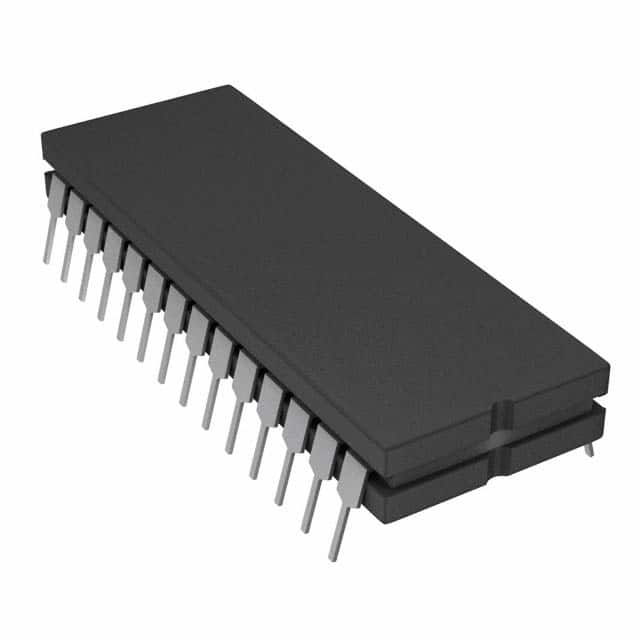
- Package: Ceramic DIP (Dual Inline Package)
- Essence: Provides high-quality analog output based on digital input signals
- Packaging/Quantity: Available in bulk packaging, quantity varies
Specifications
- Resolution: 12 bits
- Number of Channels: 1
- Input Voltage Range: 0V to Vref
- Output Voltage Range: 0V to Vref
- Operating Voltage Range: ±5V to ±15V
- Power Consumption: <1mW
- Settling Time: <10µs
- Temperature Range: -40°C to +85°C
Detailed Pin Configuration
The DAC8412AT/883C has the following pin configuration:
- VDD: Positive power supply
- VSS: Negative power supply
- VREF: Reference voltage input
- AGND: Analog ground
- AOUT: Analog output
- DIN: Digital input
- SCLK: Serial clock input
- SYNC: Chip select input
Functional Features
- High-resolution conversion from digital to analog signals
- Precise and accurate output voltage levels
- Fast settling time for rapid signal response
- Low power consumption for energy efficiency
- Wide operating voltage range for versatile applications
Advantages
- High precision and accuracy ensure reliable analog output
- Wide operating voltage range allows compatibility with various systems
- Low power consumption reduces energy usage and heat dissipation
- Fast settling time enables quick response to digital input changes
Disadvantages
- Limited to a single channel output
- Requires external reference voltage for accurate conversion
Working Principles
The DAC8412AT/883C operates by converting digital input signals into corresponding analog output voltages. It utilizes a 12-bit resolution to provide high precision and accuracy. The digital input is processed internally, and the resulting analog output voltage is generated based on the applied reference voltage. The device operates within a wide voltage range and consumes minimal power while delivering fast settling times.
Detailed Application Field Plans
The DAC8412AT/883C finds applications in various fields, including:
- Audio Systems: Provides high-quality analog audio signals for amplifiers, speakers, and other audio devices.
- Industrial Automation: Converts digital control signals into analog outputs for controlling industrial processes and equipment.
- Instrumentation: Used in measurement and testing equipment to generate precise analog signals for calibration and analysis.
- Communication Systems: Enables digital-to-analog conversion for signal processing in telecommunication systems.
- Automotive Electronics: Utilized in automotive applications such as engine control units, infotainment systems, and sensor interfaces.
Detailed and Complete Alternative Models
- DAC8411AT/883C: Similar to DAC8412AT/883C but with 11-bit resolution.
- DAC8413AT/883C: Similar to DAC8412AT/883C but with 13-bit resolution.
- DAC8414AT/883C: Similar to DAC8412AT/883C but with 14-bit resolution.
- DAC8415AT/883C: Similar to DAC8412AT/883C but with 15-bit resolution.
These alternative models offer varying resolutions to suit different application requirements.
Word count: 411
10个与DAC8412AT/883C在技术解决方案中的应用相关的常见问题及解答
What is the maximum resolution of DAC8412AT/883C?
- The maximum resolution of DAC8412AT/883C is 16 bits.What is the voltage supply range for DAC8412AT/883C?
- The voltage supply range for DAC8412AT/883C is +5V to +15V.Can DAC8412AT/883C operate in single-supply mode?
- Yes, DAC8412AT/883C can operate in single-supply mode with a voltage range of +12V to +15V.What is the typical settling time of DAC8412AT/883C?
- The typical settling time of DAC8412AT/883C is 10µs.Does DAC8412AT/883C support SPI interface?
- Yes, DAC8412AT/883C supports SPI interface for communication.What is the output voltage range of DAC8412AT/883C?
- The output voltage range of DAC8412AT/883C is 0V to Vref.Is DAC8412AT/883C suitable for industrial temperature range applications?
- Yes, DAC8412AT/883C is designed for industrial temperature range applications (-40°C to +85°C).Can DAC8412AT/883C be used in battery-powered devices?
- Yes, DAC8412AT/883C is suitable for battery-powered devices due to its low power consumption.What is the package type of DAC8412AT/883C?
- DAC8412AT/883C is available in a 24-pin ceramic DIP package.Does DAC8412AT/883C have internal reference voltage?
- No, DAC8412AT/883C requires an external reference voltage for operation.