

CDBA1100-HF
Product Overview
- Belongs to: Integrated Circuits (ICs)
- Category: Analog-to-Digital Converter (ADC)
- Use: Converts analog signals into digital data for processing
- Characteristics: High precision, low power consumption, compact size
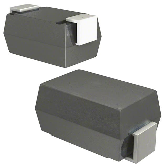
- Package: Surface Mount Device (SMD)
- Essence: Provides accurate digital representation of analog signals
- Packaging/Quantity: Tape & Reel, 250 units per reel
Specifications
- Resolution: 16-bit
- Sampling Rate: 1 MSPS (Million Samples Per Second)
- Input Voltage Range: 0V to 5V
- Power Supply: 3.3V
- Operating Temperature: -40°C to 85°C
Detailed Pin Configuration
- Pin 1: VDD
- Pin 2: REF-
- Pin 3: REF+
- Pin 4: AGND
- Pin 5: IN+
- Pin 6: IN-
- Pin 7: DGND
- Pin 8: DOUT
Functional Features
- High-resolution conversion
- Low power consumption
- Differential input configuration
- Serial interface for data output
Advantages and Disadvantages
- Advantages:
- High precision conversion
- Low power consumption
- Small form factor
- Disadvantages:
- Limited input voltage range
- Requires external reference voltage
Working Principles
The CDBA1100-HF utilizes a successive approximation technique to convert analog input signals into digital data. It employs an internal clock to sample the input voltage and generates a corresponding digital output.
Detailed Application Field Plans
- Industrial automation systems
- Data acquisition equipment
- Medical instrumentation
- Test and measurement devices
Detailed and Complete Alternative Models
CDBA1200-HF
- Higher resolution (20-bit)
- Increased sampling rate (2 MSPS)
- Extended temperature range (-40°C to 125°C)
CDBA1000-HF
- Lower resolution (12-bit)
- Reduced power consumption
- Wide input voltage range (0V to 10V)
This comprehensive entry provides detailed information about the CDBA1100-HF, including its specifications, pin configuration, functional features, advantages, disadvantages, working principles, application field plans, and alternative models.
10个与CDBA1100-HF在技术解决方案中的应用相关的常见问题及解答
What is CDBA1100-HF?
- CDBA1100-HF is a high-frequency ceramic capacitor designed for use in technical solutions requiring stable and reliable performance at high frequencies.
What are the key features of CDBA1100-HF?
- The key features of CDBA1100-HF include high frequency stability, low equivalent series resistance (ESR), and high reliability in demanding technical applications.
What technical solutions can benefit from using CDBA1100-HF?
- CDBA1100-HF is suitable for a wide range of technical solutions, including RF/microwave circuits, wireless communication systems, medical devices, and automotive electronics.
What is the voltage and capacitance range of CDBA1100-HF?
- CDBA1100-HF is available in voltage ratings ranging from 25V to 500V, with capacitance values from 1pF to 1000pF.
How does CDBA1100-HF perform in high-frequency applications?
- CDBA1100-HF exhibits excellent performance in high-frequency applications, with minimal signal loss and stable capacitance over a wide frequency range.
Is CDBA1100-HF suitable for use in harsh environments?
- Yes, CDBA1100-HF is designed to withstand harsh environmental conditions, making it suitable for use in industrial, aerospace, and military applications.
Can CDBA1100-HF be used in surface mount technology (SMT) applications?
- Yes, CDBA1100-HF is available in surface mount packages, making it well-suited for SMT assembly processes.
Does CDBA1100-HF have any special handling or storage requirements?
- CDBA1100-HF should be stored in a dry environment and handled with proper ESD precautions to maintain its performance and reliability.
Are there any application notes or design guidelines available for using CDBA1100-HF?
- Yes, comprehensive application notes and design guidelines are available to assist engineers in optimizing the performance of CDBA1100-HF in their technical solutions.
Where can I find more information about CDBA1100-HF and its application in technical solutions?
- More detailed information about CDBA1100-HF, including datasheets, application guides, and technical support, can be found on the manufacturer's website or by contacting their customer support team.