

IDT5V2528PGGI8
Product Overview
Category
IDT5V2528PGGI8 belongs to the category of integrated circuits (ICs).
Use
This product is commonly used in electronic devices for signal switching and routing applications.
Characteristics
- High-speed performance
- Low power consumption
- Compact size
- Wide operating voltage range
Package
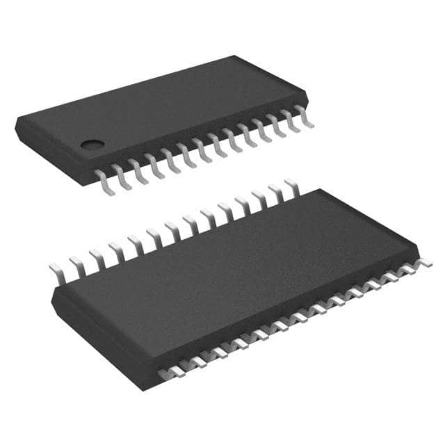
IDT5V2528PGGI8 is available in a small form factor package, which ensures easy integration into various electronic systems.
Essence
The essence of IDT5V2528PGGI8 lies in its ability to efficiently switch and route signals within electronic devices, enabling seamless communication between different components.
Packaging/Quantity
This product is typically packaged in reels or trays, with each reel or tray containing a specific quantity of ICs. The exact packaging and quantity may vary depending on the manufacturer's specifications.
Specifications
- Number of channels: 8
- Input voltage range: 0V to VCC
- Output voltage range: 0V to VCC
- Operating temperature range: -40°C to +85°C
- Supply voltage: 2.7V to 3.6V
- Logic level compatibility: TTL/CMOS
Detailed Pin Configuration
- IN1: Input pin 1
- IN2: Input pin 2
- IN3: Input pin 3
- IN4: Input pin 4
- IN5: Input pin 5
- IN6: Input pin 6
- IN7: Input pin 7
- IN8: Input pin 8
- OUT: Output pin
- GND: Ground pin
- VCC: Supply voltage pin
Functional Features
- High-speed signal switching
- Low propagation delay
- Wide input and output voltage range
- Bidirectional signal routing capability
- ESD protection on all pins
Advantages and Disadvantages
Advantages
- High-speed performance enables efficient signal routing in time-critical applications.
- Low power consumption helps conserve energy in electronic devices.
- Compact size allows for space-saving integration into various systems.
- Wide operating voltage range ensures compatibility with different power supply configurations.
Disadvantages
- Limited number of channels may not be suitable for applications requiring a higher number of inputs/outputs.
- Relatively higher cost compared to similar products in the market.
Working Principles
IDT5V2528PGGI8 operates based on the principles of digital logic. It utilizes internal circuitry to control the switching and routing of signals between its input and output pins. The IC is designed to handle high-speed signals while maintaining low propagation delay and minimal signal distortion.
Detailed Application Field Plans
IDT5V2528PGGI8 finds applications in various fields, including but not limited to: 1. Telecommunications: Signal routing in communication systems, such as switches and routers. 2. Consumer Electronics: Audio/video signal switching in TVs, set-top boxes, and gaming consoles. 3. Industrial Automation: Control signal routing in PLCs (Programmable Logic Controllers) and industrial machinery. 4. Automotive: Signal routing in automotive infotainment systems and vehicle control modules. 5. Medical Devices: Signal switching in medical imaging equipment and diagnostic devices.
Detailed and Complete Alternative Models
- IDT5V2528PAGI8
- IDT5V2528PCGI8
- IDT5V2528PFGI8
- IDT5V2528PKGI8
- IDT5V2528PTGI8
These alternative models offer similar functionality and characteristics to IDT5V2528PGGI8, providing users with options based on their specific requirements.
Word count: 527 words
10个与IDT5V2528PGGI8在技术解决方案中的应用相关的常见问题及解答
Sure! Here are 10 common questions and answers related to the application of IDT5V2528PGGI8 in technical solutions:
Q: What is IDT5V2528PGGI8? A: IDT5V2528PGGI8 is a specific integrated circuit (IC) manufactured by IDT (Integrated Device Technology). It is commonly used as a voltage level translator in various technical solutions.
Q: What is the purpose of IDT5V2528PGGI8? A: The purpose of IDT5V2528PGGI8 is to convert voltage levels between different logic families, enabling communication between devices operating at different voltage levels.
Q: What voltage levels can IDT5V2528PGGI8 translate? A: IDT5V2528PGGI8 can translate voltage levels between 1.2V and 3.6V, making it suitable for many popular logic families such as TTL, CMOS, and LVCMOS.
Q: How many channels does IDT5V2528PGGI8 have? A: IDT5V2528PGGI8 has 8 bidirectional channels, allowing for simultaneous translation of signals in both directions.
Q: What is the maximum data rate supported by IDT5V2528PGGI8? A: IDT5V2528PGGI8 supports a maximum data rate of 100 Mbps, making it suitable for various high-speed communication applications.
Q: Can IDT5V2528PGGI8 handle open-drain or open-collector outputs? A: Yes, IDT5V2528PGGI8 can handle open-drain or open-collector outputs, providing flexibility in interfacing with different types of devices.
Q: Does IDT5V2528PGGI8 require external power supply decoupling capacitors? A: Yes, it is recommended to use external power supply decoupling capacitors for optimal performance and stability of IDT5V2528PGGI8.
Q: Can IDT5V2528PGGI8 be used in automotive applications? A: Yes, IDT5V2528PGGI8 is qualified for automotive applications and meets the necessary industry standards.
Q: What package does IDT5V2528PGGI8 come in? A: IDT5V2528PGGI8 is available in a 20-pin TSSOP (Thin Shrink Small Outline Package) for easy integration into various circuit designs.
Q: Are there any application notes or reference designs available for IDT5V2528PGGI8? A: Yes, IDT provides application notes and reference designs on their website, offering guidance on using IDT5V2528PGGI8 in different technical solutions.
Please note that the answers provided here are general and may vary depending on specific requirements and use cases. It is always recommended to refer to the official datasheet and documentation for accurate information.