

LTC1448CN8#PBF
Product Overview
Category: Integrated Circuit (IC)
Use: Analog-to-Digital Converter (ADC)
Characteristics: - High precision - Low power consumption - Small form factor - Wide operating temperature range
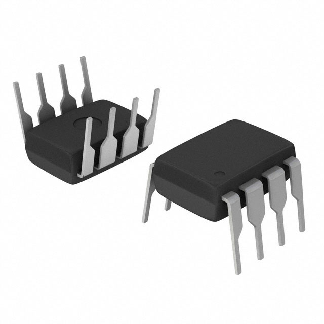
Package: 8-pin Plastic DIP (Dual In-Line Package)
Essence: The LTC1448CN8#PBF is a high-performance ADC designed for various applications that require accurate and fast analog-to-digital conversion.
Packaging/Quantity: The LTC1448CN8#PBF is available in a plastic DIP package, with a quantity of one unit per package.
Specifications
- Resolution: 12 bits
- Sampling Rate: Up to 100 kilosamples per second (ksps)
- Input Voltage Range: ±10V
- Power Supply: +5V
- Operating Temperature Range: -40°C to +85°C
- Conversion Time: 1.2µs
Pin Configuration
The LTC1448CN8#PBF has the following pin configuration:
- VCC: Power supply input (+5V)
- GND: Ground reference
- IN+: Positive analog input
- IN-: Negative analog input
- CS: Chip select input
- SCK: Serial clock input
- SDI: Serial data input
- SDO: Serial data output
Functional Features
- High-resolution conversion with low noise and distortion
- On-chip sample-and-hold circuitry for accurate signal acquisition
- Serial interface for easy integration with microcontrollers and digital systems
- Low power consumption for energy-efficient operation
- Wide input voltage range allows for versatile application scenarios
Advantages and Disadvantages
Advantages: - High precision conversion - Compact size - Versatile input voltage range - Low power consumption
Disadvantages: - Limited sampling rate compared to some other ADCs - Requires an external microcontroller or digital system for data processing and analysis
Working Principles
The LTC1448CN8#PBF operates on the principle of successive approximation. It uses a sample-and-hold circuit to capture the analog input signal, which is then converted into a digital representation using a 12-bit resolution ADC. The conversion process is controlled by the chip select input and clock signals. The resulting digital data can be accessed through the serial data output pin.
Detailed Application Field Plans
The LTC1448CN8#PBF can be used in various applications that require accurate analog-to-digital conversion, such as:
- Industrial Automation: Process control, data acquisition, and monitoring systems.
- Medical Equipment: Patient monitoring, diagnostic instruments, and biomedical devices.
- Test and Measurement: Oscilloscopes, data loggers, and signal analyzers.
- Communication Systems: Modems, telecommunication equipment, and network analyzers.
- Automotive Electronics: Engine control units, sensor interfaces, and battery management systems.
Detailed and Complete Alternative Models
- LTC1448CS8#PBF: Similar to LTC1448CN8#PBF but in a surface-mount package (SOIC).
- LTC1448IS8#PBF: Improved version with higher sampling rate and lower power consumption.
- LTC1448CMS8#PBF: Compact version with smaller form factor for space-constrained applications.
These alternative models offer similar functionality and performance characteristics, providing flexibility in choosing the most suitable option for specific application requirements.
Word count: 527 words
10个与LTC1448CN8#PBF在技术解决方案中的应用相关的常见问题及解答
Sure! Here are 10 common questions and answers related to the application of LTC1448CN8#PBF in technical solutions:
Q: What is LTC1448CN8#PBF? A: LTC1448CN8#PBF is a high-performance, low-power, 12-bit analog-to-digital converter (ADC) manufactured by Linear Technology.
Q: What is the operating voltage range of LTC1448CN8#PBF? A: The operating voltage range of LTC1448CN8#PBF is typically between 2.7V and 5.5V.
Q: What is the maximum sampling rate of LTC1448CN8#PBF? A: The maximum sampling rate of LTC1448CN8#PBF is 100ksps (thousand samples per second).
Q: What is the resolution of LTC1448CN8#PBF? A: LTC1448CN8#PBF has a resolution of 12 bits, which means it can represent analog signals with 4096 discrete levels.
Q: What is the input voltage range of LTC1448CN8#PBF? A: The input voltage range of LTC1448CN8#PBF is typically between 0V and Vref, where Vref is the reference voltage supplied to the ADC.
Q: Does LTC1448CN8#PBF support differential inputs? A: Yes, LTC1448CN8#PBF supports both single-ended and differential inputs, providing flexibility in signal acquisition.
Q: What is the power consumption of LTC1448CN8#PBF? A: The power consumption of LTC1448CN8#PBF depends on the operating conditions but is typically around 1.5mW.
Q: Can LTC1448CN8#PBF operate in a noisy environment? A: Yes, LTC1448CN8#PBF features a built-in selectable digital filter that helps reduce noise and improve signal integrity.
Q: What is the output interface of LTC1448CN8#PBF? A: LTC1448CN8#PBF has a serial SPI (Serial Peripheral Interface) output interface, which allows easy integration with microcontrollers or other digital devices.
Q: Is LTC1448CN8#PBF suitable for battery-powered applications? A: Yes, LTC1448CN8#PBF is designed to operate at low power and can be used in battery-powered applications where power efficiency is crucial.
Please note that the answers provided here are general and may vary depending on specific datasheet specifications and application requirements.