

LTC1660CGN#PBF
Product Overview
- Category: Integrated Circuit (IC)
- Use: Digital-to-Analog Converter (DAC)
- Characteristics: High precision, low power consumption
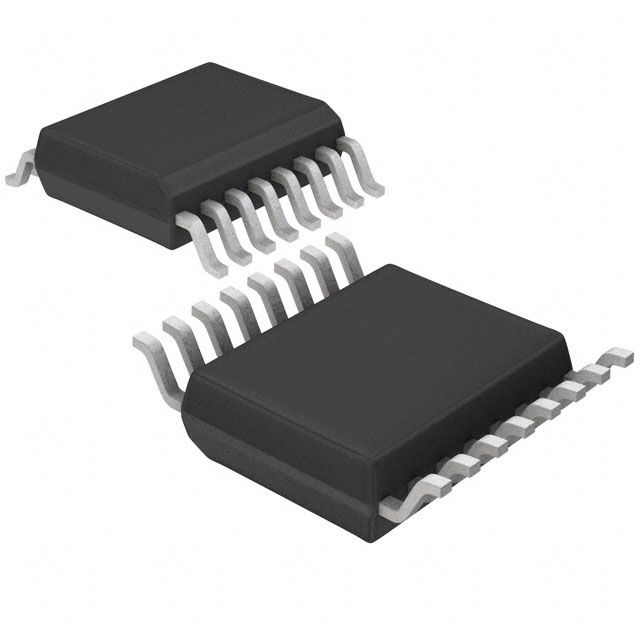
- Package: 20-pin SSOP (Shrink Small Outline Package)
- Essence: Converts digital signals into analog voltages
- Packaging/Quantity: Tape and Reel, 250 units per reel
Specifications
- Resolution: 16 bits
- Number of Channels: 1
- Supply Voltage: 2.7V to 5.5V
- Operating Temperature Range: -40°C to +85°C
- Output Voltage Range: 0V to Vref (Reference Voltage)
- DNL (Differential Non-Linearity): ±0.5 LSB (Least Significant Bit)
- INL (Integral Non-Linearity): ±1 LSB
- Power Consumption: 0.5mW (typical)
Detailed Pin Configuration
The LTC1660CGN#PBF has a total of 20 pins. The pin configuration is as follows:
- VDD - Positive supply voltage
- GND - Ground reference
- REF - Reference voltage input
- AGND - Analog ground reference
- OUT - Analog output voltage
- SDO - Serial data output
- SDI - Serial data input
- SCK - Serial clock input
- CS - Chip select input
- SHDN - Shutdown control input
- LDAC - Load DAC register control input 12-19. NC - No connection
- VREF - Reference voltage output
Functional Features
- High-resolution digital-to-analog conversion
- Low power consumption for energy-efficient applications
- Wide operating voltage range for flexibility in various systems
- Excellent linearity and accuracy for precise analog signal generation
- Serial interface for easy integration with microcontrollers and digital systems
- Shutdown control for power-saving mode
- Load DAC register control for synchronized updates of analog output
Advantages and Disadvantages
Advantages: - High precision conversion ensures accurate analog outputs - Low power consumption extends battery life in portable devices - Wide operating voltage range allows compatibility with different power supplies - Serial interface simplifies integration with digital systems - Shutdown control and load DAC register control enhance flexibility and power efficiency
Disadvantages: - Limited to single-channel operation - Higher cost compared to lower-resolution DACs - Requires external reference voltage for proper operation
Working Principles
The LTC1660CGN#PBF is a digital-to-analog converter that converts digital signals into corresponding analog voltages. It utilizes a 16-bit resolution to achieve high precision conversion. The input digital data is received through the serial data input (SDI) pin and synchronized with the serial clock (SCK) input. The chip select (CS) pin enables the device for data transfer.
The converted analog voltage is available at the OUT pin, which can be adjusted within the range of 0V to the reference voltage (Vref). The reference voltage is provided through the REF pin or an external reference source. The LTC1660CGN#PBF ensures excellent linearity and accuracy, with low differential and integral non-linearity.
Detailed Application Field Plans
The LTC1660CGN#PBF finds applications in various fields where precise analog voltage generation is required. Some potential application areas include:
- Audio Equipment: Used in audio signal processing circuits, such as digital audio mixers and equalizers.
- Instrumentation: Integrated into measurement devices, such as data loggers and oscilloscopes, for accurate signal representation.
- Industrial Automation: Employed in control systems for precise analog control of motors, valves, and actuators.
- Communication Systems: Utilized in base stations and transceivers for generating analog signals with high fidelity.
- Medical Devices: Integrated into medical equipment, such as patient monitors and diagnostic devices, for accurate signal generation.
Detailed and Complete Alternative Models
- LTC1661CGN#PBF: Similar to LTC1660CGN#PBF but with dual-channel operation.
- LTC1662CGN#PBF: 14-bit resolution DAC with similar features and characteristics.
- LTC1664CGN#PBF: Higher-resolution DAC with 18-bit resolution and improved linearity.
These alternative models offer different resolutions and channel configurations to suit specific application requirements.
Word count: 529 words
10个与LTC1660CGN#PBF在技术解决方案中的应用相关的常见问题及解答
Sure! Here are 10 common questions and answers related to the application of LTC1660CGN#PBF in technical solutions:
Q: What is LTC1660CGN#PBF? A: LTC1660CGN#PBF is a specific model number for a digital-to-analog converter (DAC) chip manufactured by Linear Technology Corporation.
Q: What is the purpose of LTC1660CGN#PBF? A: The LTC1660CGN#PBF DAC chip is used to convert digital signals into analog voltages, making it useful in various applications such as audio systems, instrumentation, and control systems.
Q: What is the resolution of LTC1660CGN#PBF? A: LTC1660CGN#PBF has a resolution of 16 bits, meaning it can represent 2^16 (65,536) different voltage levels.
Q: What is the operating voltage range of LTC1660CGN#PBF? A: LTC1660CGN#PBF operates within a voltage range of 2.7V to 5.5V.
Q: How many channels does LTC1660CGN#PBF have? A: LTC1660CGN#PBF is a single-channel DAC, meaning it can generate one analog output voltage at a time.
Q: What is the maximum output voltage range of LTC1660CGN#PBF? A: The maximum output voltage range of LTC1660CGN#PBF is determined by the reference voltage applied to it. It can typically cover the full range from 0V to the reference voltage.
Q: Does LTC1660CGN#PBF support serial communication interfaces? A: Yes, LTC1660CGN#PBF supports serial communication interfaces such as SPI (Serial Peripheral Interface) and I2C (Inter-Integrated Circuit).
Q: Can LTC1660CGN#PBF be used in both single-ended and differential output configurations? A: Yes, LTC1660CGN#PBF can be configured for both single-ended and differential output modes, providing flexibility in different applications.
Q: What is the settling time of LTC1660CGN#PBF? A: The settling time of LTC1660CGN#PBF refers to the time it takes for the output voltage to reach a specified accuracy after a change in the digital input. It typically ranges from a few microseconds to tens of microseconds.
Q: Are there any evaluation boards or development kits available for LTC1660CGN#PBF? A: Yes, Linear Technology Corporation provides evaluation boards and development kits that include LTC1660CGN#PBF, allowing engineers to easily test and prototype their designs using this DAC chip.
Please note that the answers provided here are general and may vary depending on specific datasheet specifications and application requirements.