

LTC1665IGN#PBF
Product Overview
Category: Integrated Circuit (IC)
Use: Digital-to-Analog Converter (DAC)
Characteristics: - High-resolution DAC - Low power consumption - Wide operating voltage range - Small package size - Serial interface for easy integration
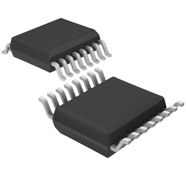
Package: 16-pin SSOP (Shrink Small Outline Package)
Essence: The LTC1665IGN#PBF is a high-performance DAC designed for various applications requiring precise analog voltage outputs.
Packaging/Quantity: Available in tape and reel packaging, with a quantity of 250 units per reel.
Specifications
- Resolution: 16 bits
- Supply Voltage Range: 2.7V to 5.5V
- Output Voltage Range: 0V to Vref
- Operating Temperature Range: -40°C to +85°C
- DNL (Differential Non-Linearity): ±1 LSB (max)
- INL (Integral Non-Linearity): ±2 LSB (max)
- Power Consumption: 0.6mW (typ) at 3V supply
Pin Configuration
The LTC1665IGN#PBF has the following pin configuration:
```
| | | 1 2 3 4 5 6 7 8 | |_______________________________________|
- VDD
- SDO
- SCK
- CS
- GND
- REF
- AGND
- OUTA ```
Functional Features
- High-resolution digital-to-analog conversion
- Serial interface for easy communication with microcontrollers or other digital devices
- Low power consumption for energy-efficient applications
- Wide operating voltage range allows for flexibility in power supply selection
- Small package size enables compact designs
Advantages and Disadvantages
Advantages: - High resolution provides accurate analog voltage outputs - Low power consumption extends battery life in portable devices - Serial interface simplifies integration with digital systems - Wide operating voltage range enhances compatibility with different power supplies
Disadvantages: - Limited output voltage range may not be suitable for applications requiring higher voltage levels - 16-pin SSOP package may require additional space on the PCB compared to smaller packages
Working Principles
The LTC1665IGN#PBF operates by converting digital input signals into precise analog voltage outputs. It utilizes a 16-bit resolution DAC, which allows for high accuracy in generating analog voltages. The serial interface enables easy communication with microcontrollers or other digital devices, making it suitable for various applications.
Detailed Application Field Plans
The LTC1665IGN#PBF can be used in a wide range of applications, including but not limited to: 1. Audio equipment: Providing accurate analog voltage outputs for audio signal processing. 2. Industrial automation: Generating precise control signals for industrial machinery. 3. Test and measurement instruments: Producing calibrated analog signals for testing purposes. 4. Communication systems: Generating analog voltage references for signal conditioning. 5. Automotive electronics: Providing accurate voltage outputs for automotive control systems.
Detailed and Complete Alternative Models
- LTC1666IGN#PBF: Similar to LTC1665IGN#PBF but with an extended temperature range (-40°C to +125°C).
- LTC1667IGN#PBF: Higher resolution (18 bits) DAC with similar features and characteristics.
- LTC1668IGN#PBF: Lower power consumption version of LTC1665IGN#PBF with reduced supply voltage range (2.7V to 3.6V).
These alternative models offer similar functionality and can be considered based on specific application requirements.
Word count: 455 words
10个与LTC1665IGN#PBF在技术解决方案中的应用相关的常见问题及解答
Sure! Here are 10 common questions and answers related to the application of LTC1665IGN#PBF in technical solutions:
Q: What is LTC1665IGN#PBF? A: LTC1665IGN#PBF is a specific model number for a digital-to-analog converter (DAC) manufactured by Linear Technology (now part of Analog Devices). It is used to convert digital signals into analog voltages.
Q: What is the operating voltage range of LTC1665IGN#PBF? A: The operating voltage range of LTC1665IGN#PBF is typically between 2.7V and 5.5V.
Q: How many bits does LTC1665IGN#PBF have? A: LTC1665IGN#PBF is a 16-bit DAC, meaning it can provide 2^16 (65,536) different output voltage levels.
Q: What is the maximum output voltage range of LTC1665IGN#PBF? A: The maximum output voltage range of LTC1665IGN#PBF is typically between 0V and Vref, where Vref is the reference voltage provided to the DAC.
Q: Can LTC1665IGN#PBF be used in both single-ended and differential mode? A: Yes, LTC1665IGN#PBF can be used in both single-ended and differential mode, depending on the application requirements.
Q: What is the typical settling time of LTC1665IGN#PBF? A: The typical settling time of LTC1665IGN#PBF is around 10µs, which refers to the time it takes for the output voltage to reach within a specified error band after a change in the input code.
Q: Does LTC1665IGN#PBF have an internal reference voltage? A: No, LTC1665IGN#PBF does not have an internal reference voltage. An external reference voltage must be provided to the DAC.
Q: Can LTC1665IGN#PBF operate in a low-power mode? A: Yes, LTC1665IGN#PBF has a power-down mode that allows it to consume very low power when not actively converting digital signals.
Q: What is the typical output impedance of LTC1665IGN#PBF? A: The typical output impedance of LTC1665IGN#PBF is around 0.1 ohms, which means it can drive loads with relatively low impedance.
Q: Are there any evaluation boards or development kits available for LTC1665IGN#PBF? A: Yes, Analog Devices provides evaluation boards and development kits for LTC1665IGN#PBF, which can help users quickly prototype and test their applications.
Please note that the answers provided here are general and may vary depending on specific datasheet specifications and application requirements.