

LTC2601CDD-1#PBF
Product Overview
Category
The LTC2601CDD-1#PBF belongs to the category of digital-to-analog converters (DACs).
Use
It is primarily used for converting digital signals into analog voltage outputs.
Characteristics
- High precision and accuracy
- Low power consumption
- Small form factor
- Wide operating temperature range
- Easy integration with microcontrollers and other digital systems
Package
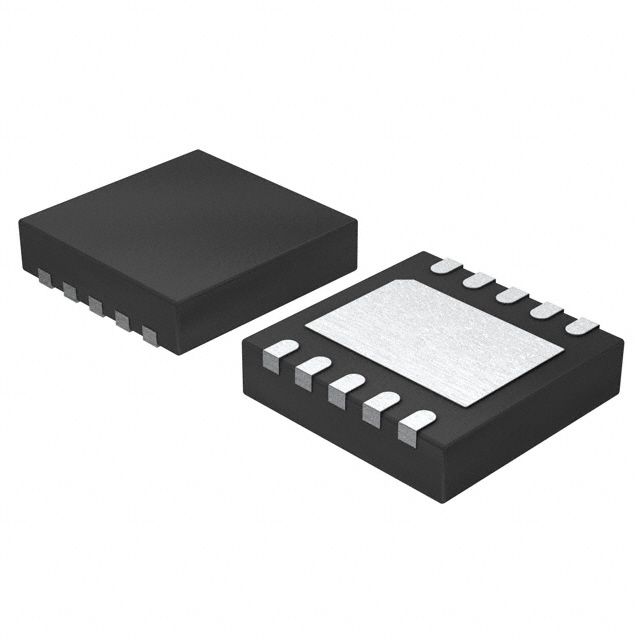
The LTC2601CDD-1#PBF comes in a compact DFN package, which ensures efficient heat dissipation and ease of mounting on circuit boards.
Essence
The essence of the LTC2601CDD-1#PBF lies in its ability to provide accurate analog voltage outputs based on digital input signals.
Packaging/Quantity
This product is typically packaged in reels or tubes, with a quantity of 250 units per reel/tube.
Specifications
- Resolution: 16 bits
- Output Voltage Range: 0V to Vref
- Supply Voltage Range: 2.7V to 5.5V
- Operating Temperature Range: -40°C to 85°C
- Integral Non-Linearity (INL): ±1 LSB (max)
- Differential Non-Linearity (DNL): ±1 LSB (max)
- Power Consumption: 0.5mW (typ)
Detailed Pin Configuration
The LTC2601CDD-1#PBF has the following pin configuration:
- VDD: Power supply voltage
- GND: Ground reference
- SDA: Serial data input
- SCL: Serial clock input
- A0: Address input bit 0
- A1: Address input bit 1
- REF: Reference voltage input
- OUT: Analog voltage output
Functional Features
- High-resolution digital-to-analog conversion
- I2C-compatible serial interface for easy communication with microcontrollers
- On-chip reference voltage generator for simplified circuit design
- Power-on reset ensures reliable startup and initialization
- Low glitch impulse for minimal output voltage disturbance during transitions
Advantages and Disadvantages
Advantages
- High precision and accuracy in analog voltage output
- Low power consumption for energy-efficient applications
- Compact form factor allows for space-saving designs
- Wide operating temperature range enables usage in various environments
- Easy integration with digital systems simplifies overall circuit design
Disadvantages
- Limited output voltage range (0V to Vref)
- Relatively high cost compared to lower-resolution DACs
- Requires an external reference voltage source
Working Principles
The LTC2601CDD-1#PBF operates based on the principle of binary-weighted resistor networks. It converts digital input signals into corresponding analog voltages using a combination of switches and resistors. The digital input is processed by an internal digital-to-analog converter, which generates the desired analog voltage output.
Detailed Application Field Plans
The LTC2601CDD-1#PBF finds applications in various fields, including:
- Industrial automation: Precise control of analog actuators and sensors.
- Test and measurement equipment: Accurate signal generation and calibration.
- Audio equipment: High-fidelity audio signal processing and amplification.
- Instrumentation and control systems: Analog signal conditioning and control.
- Automotive electronics: Voltage control for automotive subsystems.
Detailed and Complete Alternative Models
- LTC2600CDD-1#PBF: 16-bit digital-to-analog converter with similar specifications and features.
- AD5662BRMZ-1RL7: 16-bit nanoDAC with I2C interface and comparable performance.
- MCP4725A0T-E/CH: 12-bit DAC with I2C interface, suitable for lower-resolution applications.
These alternative models offer similar functionality and can be considered based on specific application requirements.
Word count: 511 words
10个与LTC2601CDD-1#PBF在技术解决方案中的应用相关的常见问题及解答
Sure! Here are 10 common questions and answers related to the application of LTC2601CDD-1#PBF in technical solutions:
Q1: What is LTC2601CDD-1#PBF? A1: LTC2601CDD-1#PBF is a digital-to-analog converter (DAC) manufactured by Linear Technology (now part of Analog Devices). It converts digital signals into analog voltages.
Q2: What is the resolution of LTC2601CDD-1#PBF? A2: LTC2601CDD-1#PBF has a resolution of 16 bits, which means it can represent 2^16 (65,536) different voltage levels.
Q3: What is the supply voltage range for LTC2601CDD-1#PBF? A3: The supply voltage range for LTC2601CDD-1#PBF is typically between 2.7V and 5.5V.
Q4: What is the interface used to communicate with LTC2601CDD-1#PBF? A4: LTC2601CDD-1#PBF uses an I2C (Inter-Integrated Circuit) interface for communication with microcontrollers or other devices.
Q5: Can LTC2601CDD-1#PBF operate in both single-ended and differential modes? A5: Yes, LTC2601CDD-1#PBF can operate in both single-ended and differential modes, providing flexibility in various applications.
Q6: What is the typical settling time of LTC2601CDD-1#PBF? A6: The typical settling time of LTC2601CDD-1#PBF is around 6 microseconds, ensuring fast response in dynamic applications.
Q7: Does LTC2601CDD-1#PBF have an internal reference voltage? A7: No, LTC2601CDD-1#PBF does not have an internal reference voltage. An external reference voltage is required for accurate conversions.
Q8: Can LTC2601CDD-1#PBF be used in battery-powered applications? A8: Yes, LTC2601CDD-1#PBF can be used in battery-powered applications due to its low power consumption and wide supply voltage range.
Q9: What is the temperature range of LTC2601CDD-1#PBF? A9: LTC2601CDD-1#PBF has an operating temperature range of -40°C to +85°C, making it suitable for a wide range of environments.
Q10: Are there any evaluation boards or development kits available for LTC2601CDD-1#PBF? A10: Yes, Analog Devices provides evaluation boards and development kits for LTC2601CDD-1#PBF, which can help in prototyping and testing applications.
Please note that the answers provided here are general and may vary depending on specific datasheet specifications and application requirements.