

LTC2606CDD#PBF
Product Overview
Category
The LTC2606CDD#PBF belongs to the category of digital-to-analog converters (DACs).
Use
It is primarily used for converting digital signals into analog voltage outputs.
Characteristics
- High precision and accuracy
- Low power consumption
- Wide operating temperature range
- Small form factor
- Easy integration into various systems
Package
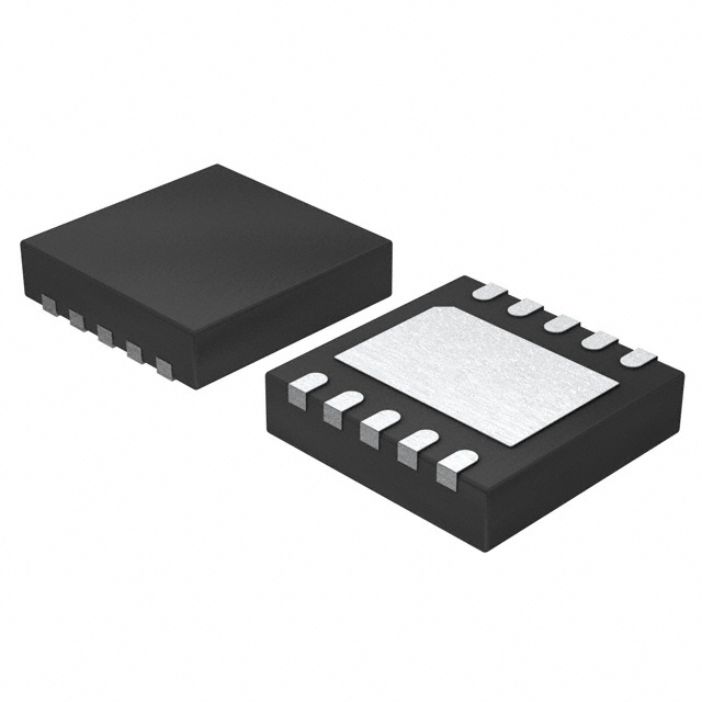
The LTC2606CDD#PBF comes in a DFN (Dual Flat No-Lead) package.
Essence
The essence of LTC2606CDD#PBF lies in its ability to provide accurate analog voltage outputs based on digital input signals.
Packaging/Quantity
This product is typically packaged in reels or tubes, with a quantity of 250 units per reel/tube.
Specifications
- Resolution: 16 bits
- Supply Voltage Range: 2.7V to 5.5V
- Output Voltage Range: 0V to VREF
- Operating Temperature Range: -40°C to +85°C
- Integral Nonlinearity (INL): ±1 LSB (max)
- Differential Nonlinearity (DNL): ±1 LSB (max)
- Power Consumption: 0.5mW (typ)
Detailed Pin Configuration
The LTC2606CDD#PBF has the following pin configuration:
- VDD: Power supply input
- GND: Ground reference
- SDA: Serial data input
- SCL: Serial clock input
- A0: Address bit 0
- A1: Address bit 1
- REF: Reference voltage input
- OUT: Analog voltage output
Functional Features
- High-resolution digital-to-analog conversion
- I2C-compatible serial interface for easy communication
- Programmable output voltage range
- Power-on reset to ensure reliable startup
- Low glitch impulse for minimal noise generation
Advantages and Disadvantages
Advantages
- High precision and accuracy in analog voltage outputs
- Wide operating temperature range allows for versatile applications
- Low power consumption for energy-efficient designs
- Small form factor enables space-constrained installations
- Easy integration into various systems due to I2C compatibility
Disadvantages
- Limited output voltage range compared to some other DACs
- Relatively higher cost compared to lower-resolution DACs
Working Principles
The LTC2606CDD#PBF operates based on the principle of digital-to-analog conversion. It takes digital input signals and converts them into corresponding analog voltage outputs. This is achieved through a combination of internal circuitry and algorithms that accurately translate the digital data into precise analog voltages.
Detailed Application Field Plans
The LTC2606CDD#PBF finds applications in various fields, including but not limited to: 1. Industrial automation and control systems 2. Test and measurement equipment 3. Audio and video processing devices 4. Medical instrumentation 5. Automotive electronics 6. Telecommunications infrastructure
Detailed and Complete Alternative Models
- LTC2607: Similar to LTC2606CDD#PBF but with additional features such as integrated reference voltage and more output channels.
- MAX5216: 16-bit DAC with similar performance characteristics and I2C interface.
- AD5669: Another 16-bit DAC with low power consumption and flexible output voltage range.
These alternative models provide similar functionality and can be considered as alternatives to LTC2606CDD#PBF depending on specific requirements and design considerations.
Word count: 511 words
10个与LTC2606CDD#PBF在技术解决方案中的应用相关的常见问题及解答
Sure! Here are 10 common questions and answers related to the application of LTC2606CDD#PBF in technical solutions:
Q: What is LTC2606CDD#PBF? A: LTC2606CDD#PBF is a digital-to-analog converter (DAC) chip manufactured by Linear Technology (now part of Analog Devices). It is used to convert digital signals into analog voltages.
Q: What is the resolution of LTC2606CDD#PBF? A: LTC2606CDD#PBF has a resolution of 16 bits, which means it can provide 65,536 discrete voltage levels.
Q: What is the operating voltage range of LTC2606CDD#PBF? A: The operating voltage range of LTC2606CDD#PBF is typically between 2.7V and 5.5V.
Q: How many channels does LTC2606CDD#PBF have? A: LTC2606CDD#PBF has six independent DAC channels, allowing you to control up to six different analog outputs.
Q: What is the interface used to communicate with LTC2606CDD#PBF? A: LTC2606CDD#PBF uses an I2C-compatible serial interface for communication with a microcontroller or other digital devices.
Q: Can LTC2606CDD#PBF operate in both unipolar and bipolar modes? A: Yes, LTC2606CDD#PBF can be configured to operate in either unipolar mode (0V to Vref) or bipolar mode (-Vref/2 to +Vref/2).
Q: What is the settling time of LTC2606CDD#PBF? A: The settling time of LTC2606CDD#PBF is typically 10μs, which refers to the time it takes for the output voltage to reach within a specified error band after a change in the digital input.
Q: Can LTC2606CDD#PBF be used in precision applications? A: Yes, LTC2606CDD#PBF is designed for precision applications and offers low integral nonlinearity (INL) and differential nonlinearity (DNL) specifications.
Q: What is the power consumption of LTC2606CDD#PBF? A: The power consumption of LTC2606CDD#PBF depends on the operating conditions but is typically around 1mW.
Q: Are there any evaluation boards or development kits available for LTC2606CDD#PBF? A: Yes, Analog Devices provides evaluation boards and development kits that can be used to quickly prototype and test LTC2606CDD#PBF in various applications.
Please note that the specific details and specifications may vary, so it's always recommended to refer to the datasheet or consult with the manufacturer for accurate information.