

LTC2630HSC6-LZ10#TRMPBF
Product Overview
- Category: Integrated Circuit (IC)
- Use: Digital-to-Analog Converter (DAC)
- Characteristics:
- High precision
- Low power consumption
- Small package size
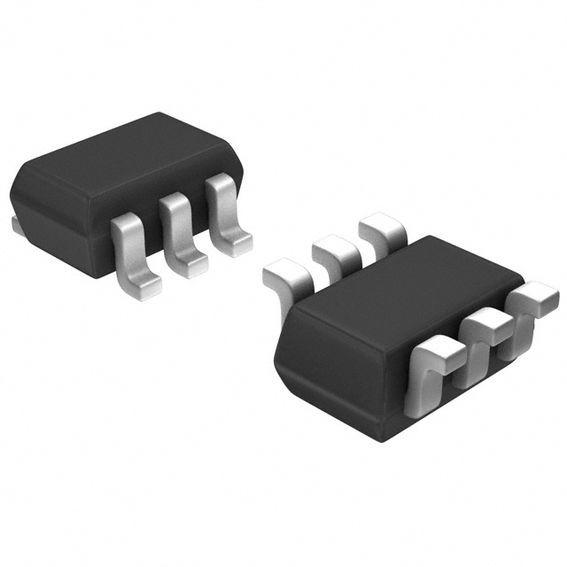
- Package: SOT-23-6
- Essence: LTC2630HSC6-LZ10#TRMPBF is a high-performance DAC that converts digital signals into analog voltages with high precision and low power consumption. It comes in a small SOT-23-6 package.
- Packaging/Quantity: The LTC2630HSC6-LZ10#TRMPBF is typically sold in reels of 2500 units.
Specifications
- Resolution: 10 bits
- Number of Channels: 1
- Interface Type: Serial, SPI-compatible
- Supply Voltage Range: 2.7V to 5.5V
- Output Voltage Range: 0V to Vref
- Operating Temperature Range: -40°C to +85°C
Pin Configuration
The LTC2630HSC6-LZ10#TRMPBF has the following pin configuration:
___________
      |           |
   NC |1         6| VDD
   CS |2         5| SCK
  SDO |3         4| SDI
      |___________|
- Pin 1 (NC): No connection
- Pin 2 (CS): Chip Select input
- Pin 3 (SDO): Serial Data Output
- Pin 4 (SDI): Serial Data Input
- Pin 5 (SCK): Serial Clock Input
- Pin 6 (VDD): Power supply voltage
Functional Features
- High accuracy and resolution: The LTC2630HSC6-LZ10#TRMPBF provides 10-bit resolution, allowing for precise analog voltage generation.
- Low power consumption: This DAC operates with low power requirements, making it suitable for battery-powered applications.
- Small package size: The SOT-23-6 package offers a compact form factor, enabling space-constrained designs.
Advantages and Disadvantages
Advantages
- High precision and accuracy
- Low power consumption
- Compact package size
- Wide operating temperature range
Disadvantages
- Limited number of channels (only 1 channel)
- Requires an external reference voltage (Vref)
Working Principles
The LTC2630HSC6-LZ10#TRMPBF utilizes a serial interface to receive digital input data. It then converts this digital data into an analog voltage output based on the applied reference voltage (Vref). The internal circuitry ensures high precision and accuracy in the conversion process.
Detailed Application Field Plans
The LTC2630HSC6-LZ10#TRMPBF is commonly used in various applications that require accurate analog voltage generation. Some potential application fields include:
- Industrial automation: Control systems that require precise analog signals for motor control, valve control, or sensor calibration.
- Test and measurement equipment: Used in signal generators, waveform synthesizers, or calibration devices.
- Audio equipment: Digital-to-analog conversion in audio amplifiers, mixers, or musical instruments.
- Communication systems: Generating analog signals for modulation, demodulation, or frequency synthesis.
Detailed and Complete Alternative Models
- LTC2630HSC6-LZ12#TRMPBF: Similar to LTC2630HSC6-LZ10#TRMPBF but with 12-bit resolution.
- LTC2630HSC6-LZ8#TRMPBF: Similar to LTC2630HSC6-LZ10#TRMPBF but with 8-bit resolution.
- LTC2630HSC6-LZ16#TRMPBF: Similar to LTC2630HSC6-LZ10#TRMPBF but with 16-bit resolution.
These alternative models offer different resolutions to suit specific application requirements.
Word count: 408 words
10个与LTC2630HSC6-LZ10#TRMPBF在技术解决方案中的应用相关的常见问题及解答
Sure! Here are 10 common questions and answers related to the application of LTC2630HSC6-LZ10#TRMPBF in technical solutions:
Q: What is LTC2630HSC6-LZ10#TRMPBF? A: LTC2630HSC6-LZ10#TRMPBF is a digital-to-analog converter (DAC) manufactured by Linear Technology (now part of Analog Devices). It is a 10-bit DAC with a high-speed SPI interface.
Q: What is the operating voltage range of LTC2630HSC6-LZ10#TRMPBF? A: The operating voltage range of LTC2630HSC6-LZ10#TRMPBF is from 2.7V to 5.5V.
Q: What is the resolution of LTC2630HSC6-LZ10#TRMPBF? A: LTC2630HSC6-LZ10#TRMPBF has a resolution of 10 bits, which means it can represent 1024 different output voltage levels.
Q: How fast can LTC2630HSC6-LZ10#TRMPBF update its output voltage? A: LTC2630HSC6-LZ10#TRMPBF has a settling time of 6µs, which means it can update its output voltage within that time frame.
Q: Can LTC2630HSC6-LZ10#TRMPBF be used in both single-ended and differential mode? A: Yes, LTC2630HSC6-LZ10#TRMPBF can be used in both single-ended and differential mode, depending on the application requirements.
Q: What is the maximum output voltage range of LTC2630HSC6-LZ10#TRMPBF? A: The maximum output voltage range of LTC2630HSC6-LZ10#TRMPBF is from 0V to VREF, where VREF is the reference voltage supplied to the DAC.
Q: Can LTC2630HSC6-LZ10#TRMPBF operate in a power-down mode? A: Yes, LTC2630HSC6-LZ10#TRMPBF has a power-down mode that allows it to consume very low power when not in use.
Q: What is the temperature range for LTC2630HSC6-LZ10#TRMPBF? A: LTC2630HSC6-LZ10#TRMPBF has an operating temperature range of -40°C to +125°C.
Q: Does LTC2630HSC6-LZ10#TRMPBF have any built-in error correction mechanisms? A: Yes, LTC2630HSC6-LZ10#TRMPBF incorporates a proprietary Dynamic Element Matching (DEM) technology that helps reduce errors and improve linearity.
Q: What are some typical applications of LTC2630HSC6-LZ10#TRMPBF? A: LTC2630HSC6-LZ10#TRMPBF is commonly used in various applications such as industrial automation, instrumentation, data acquisition systems, motor control, and audio equipment.
Please note that the answers provided here are general and may vary depending on specific datasheet specifications and application requirements.