

LTC2631CTS8-HZ10#TRMPBF
Product Overview
Category: Integrated Circuit (IC)
Use: Digital-to-Analog Converter (DAC)
Characteristics: - High precision - Low power consumption - Small form factor - Wide operating temperature range
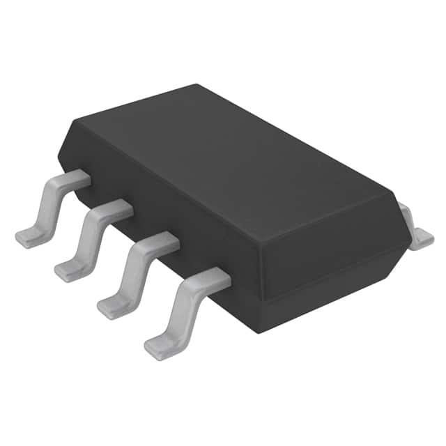
Package: TSOT-23-8
Essence: The LTC2631CTS8-HZ10#TRMPBF is a high-performance DAC that converts digital signals into analog voltages with exceptional accuracy and low power consumption.
Packaging/Quantity: This product is available in tape and reel packaging, with 3000 units per reel.
Specifications
- Resolution: 10 bits
- Number of Channels: 1
- Output Type: Voltage
- Interface Type: I2C
- Supply Voltage: 2.7V to 5.5V
- Operating Temperature Range: -40°C to +125°C
- DNL (Differential Nonlinearity): ±0.5 LSB (max)
- INL (Integral Nonlinearity): ±1 LSB (max)
- Power Consumption: 0.5mW (typ) at 3.3V
Pin Configuration
The LTC2631CTS8-HZ10#TRMPBF has the following pin configuration:
```
| | --| VDD GND |-- Power Supply --| SDA SCL |-- I2C Interface --| AOUT |-- Analog Output |___________| ```
Functional Features
- High precision digital-to-analog conversion
- Low power consumption for energy-efficient applications
- Compact size for space-constrained designs
- Wide operating temperature range for versatile usage scenarios
- I2C interface for easy integration with microcontrollers and other digital systems
Advantages and Disadvantages
Advantages: - High precision conversion ensures accurate analog output - Low power consumption extends battery life in portable devices - Small form factor allows for flexible placement in compact designs - Wide operating temperature range enables usage in extreme environments
Disadvantages: - Limited to a single channel output - Requires an I2C interface for communication
Working Principles
The LTC2631CTS8-HZ10#TRMPBF operates by receiving digital input signals through the I2C interface. These digital signals are then converted into corresponding analog voltages using a high-precision DAC circuitry. The resulting analog voltage is available at the AOUT pin, which can be used as an input for various analog applications.
Detailed Application Field Plans
The LTC2631CTS8-HZ10#TRMPBF finds applications in various fields, including but not limited to: - Industrial automation - Test and measurement equipment - Audio systems - Communication devices - Medical instruments
Detailed and Complete Alternative Models
- LTC2631CTS8-HZ12#TRMPBF: 12-bit resolution DAC with similar features
- LTC2631CTS8-HZ8#TRMPBF: 8-bit resolution DAC with similar features
- LTC2631HTS8-HZ10#TRMPBF: High-temperature version with 10-bit resolution
These alternative models provide different resolution options and may suit specific application requirements.
Word count: 346 words
10个与LTC2631CTS8-HZ10#TRMPBF在技术解决方案中的应用相关的常见问题及解答
Sure! Here are 10 common questions and answers related to the application of LTC2631CTS8-HZ10#TRMPBF in technical solutions:
Q1: What is LTC2631CTS8-HZ10#TRMPBF? A1: LTC2631CTS8-HZ10#TRMPBF is a specific model of digital-to-analog converter (DAC) manufactured by Linear Technology (now part of Analog Devices). It is designed for precision voltage output applications.
Q2: What is the resolution of LTC2631CTS8-HZ10#TRMPBF? A2: The LTC2631CTS8-HZ10#TRMPBF has a resolution of 10 bits, meaning it can represent 2^10 (1024) different voltage levels.
Q3: What is the supply voltage range for LTC2631CTS8-HZ10#TRMPBF? A3: The supply voltage range for LTC2631CTS8-HZ10#TRMPBF is typically between 2.7V and 5.5V.
Q4: What is the output voltage range of LTC2631CTS8-HZ10#TRMPBF? A4: The output voltage range of LTC2631CTS8-HZ10#TRMPBF depends on the reference voltage used. It can be programmed to output any voltage within the range of the reference voltage.
Q5: How can I communicate with LTC2631CTS8-HZ10#TRMPBF? A5: LTC2631CTS8-HZ10#TRMPBF supports various communication interfaces such as I2C and SPI. You can use these interfaces to send commands and data to the DAC.
Q6: Can LTC2631CTS8-HZ10#TRMPBF operate in both single-ended and differential modes? A6: Yes, LTC2631CTS8-HZ10#TRMPBF can operate in both single-ended and differential modes, depending on the application requirements.
Q7: What is the settling time of LTC2631CTS8-HZ10#TRMPBF? A7: The settling time of LTC2631CTS8-HZ10#TRMPBF refers to the time it takes for the output voltage to reach a specified accuracy after a change in the input code. It typically ranges from a few microseconds to tens of microseconds.
Q8: Can I use LTC2631CTS8-HZ10#TRMPBF in battery-powered applications? A8: Yes, LTC2631CTS8-HZ10#TRMPBF is suitable for battery-powered applications as it has a low supply voltage requirement and low power consumption.
Q9: Is LTC2631CTS8-HZ10#TRMPBF suitable for high-precision applications? A9: Yes, LTC2631CTS8-HZ10#TRMPBF is designed for high-precision applications. It offers excellent linearity, low noise, and low drift characteristics.
Q10: Are there any evaluation boards or development kits available for LTC2631CTS8-HZ10#TRMPBF? A10: Yes, Analog Devices provides evaluation boards and development kits for LTC2631CTS8-HZ10#TRMPBF, which can help you quickly prototype and test your designs.
Please note that the answers provided here are general and may vary based on specific datasheet information and application requirements.