

LTC2631HTS8-LZ10#TRMPBF
Product Overview
- Category: Integrated Circuit (IC)
- Use: Digital-to-Analog Converter (DAC)
- Characteristics: High precision, low power consumption
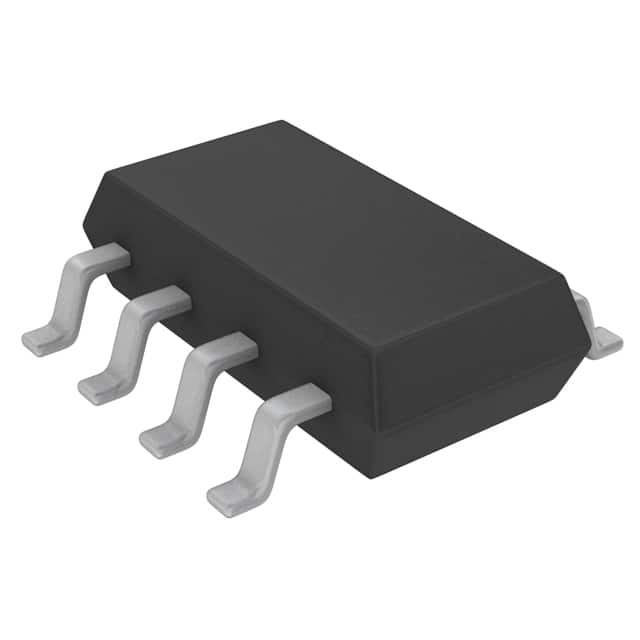
- Package: TSOT-8
- Essence: Converts digital signals to analog voltages
- Packaging/Quantity: Tape and Reel, 3000 units per reel
Specifications
- Resolution: 10 bits
- Number of Channels: 1
- Interface Type: I2C
- Supply Voltage: 2.7V to 5.5V
- Operating Temperature Range: -40°C to +85°C
- Output Voltage Range: 0V to VREF
Detailed Pin Configuration
The LTC2631HTS8-LZ10#TRMPBF has the following pin configuration:
- VDD: Power supply voltage
- SDA: Serial Data Input/Output
- SCL: Serial Clock Input
- A0: Address Input
- GND: Ground
- REF: Reference Voltage Input
- VOUT: Analog Output
- NC: No Connection
Functional Features
- High accuracy and resolution for precise analog output
- Low power consumption for energy-efficient applications
- Wide operating voltage range for versatile usage
- I2C interface allows easy integration with microcontrollers
- On-chip reference voltage simplifies external circuitry
Advantages and Disadvantages
Advantages
- High precision and resolution ensure accurate analog outputs.
- Low power consumption makes it suitable for battery-powered devices.
- Versatile operating voltage range enables compatibility with various systems.
- I2C interface provides easy control and communication with other devices.
- On-chip reference voltage reduces the need for external components.
Disadvantages
- Limited to a single channel output.
- Requires an external reference voltage for accurate conversions.
Working Principles
The LTC2631HTS8-LZ10#TRMPBF is a digital-to-analog converter that converts digital signals into corresponding analog voltages. It utilizes a 10-bit resolution to provide high precision outputs. The device operates through the I2C interface, allowing users to send digital data to control the analog output voltage. The on-chip reference voltage ensures accurate conversions within the specified output voltage range.
Detailed Application Field Plans
The LTC2631HTS8-LZ10#TRMPBF finds applications in various fields, including:
- Industrial Automation: Precise control of analog signals in industrial processes.
- Test and Measurement Equipment: Generating accurate analog signals for testing purposes.
- Audio Systems: Producing high-quality audio signals with low distortion.
- Instrumentation: Providing precise voltage references for measurement instruments.
- Communication Systems: Generating analog signals for modulation and demodulation.
Detailed and Complete Alternative Models
- LTC2631CTS8-LZ10#TRMPBF: Similar specifications but in a different package (TSOT-8).
- LTC2631IMS8-LZ10#PBF: Similar specifications but in a different package (MSOP-8).
- LTC2631HMSE-LZ10#TRPBF: Higher resolution (12 bits) with similar characteristics.
(Note: This list is not exhaustive and other alternative models may exist.)
Word count: 408 words
10个与LTC2631HTS8-LZ10#TRMPBF在技术解决方案中的应用相关的常见问题及解答
Sure! Here are 10 common questions and answers related to the application of LTC2631HTS8-LZ10#TRMPBF in technical solutions:
Q1: What is LTC2631HTS8-LZ10#TRMPBF? A1: LTC2631HTS8-LZ10#TRMPBF is a specific model of digital-to-analog converter (DAC) manufactured by Linear Technology (now part of Analog Devices). It is designed for precision voltage output applications.
Q2: What is the resolution of LTC2631HTS8-LZ10#TRMPBF? A2: LTC2631HTS8-LZ10#TRMPBF has a resolution of 10 bits, meaning it can provide 1024 different voltage levels.
Q3: What is the supply voltage range for LTC2631HTS8-LZ10#TRMPBF? A3: The supply voltage range for LTC2631HTS8-LZ10#TRMPBF is typically between 2.7V and 5.5V.
Q4: What is the output voltage range of LTC2631HTS8-LZ10#TRMPBF? A4: The output voltage range of LTC2631HTS8-LZ10#TRMPBF is determined by the reference voltage used. It can be programmed to output any voltage within the reference voltage range.
Q5: How can I communicate with LTC2631HTS8-LZ10#TRMPBF? A5: LTC2631HTS8-LZ10#TRMPBF supports both I2C and SPI communication protocols, allowing you to easily interface it with microcontrollers or other digital devices.
Q6: Can LTC2631HTS8-LZ10#TRMPBF operate in a single-ended or differential mode? A6: LTC2631HTS8-LZ10#TRMPBF can operate in both single-ended and differential mode, providing flexibility in various applications.
Q7: What is the settling time of LTC2631HTS8-LZ10#TRMPBF? A7: The settling time of LTC2631HTS8-LZ10#TRMPBF is typically around 4.5µs, ensuring fast and accurate voltage output.
Q8: Can I use LTC2631HTS8-LZ10#TRMPBF in battery-powered applications? A8: Yes, LTC2631HTS8-LZ10#TRMPBF has a low power consumption and wide supply voltage range, making it suitable for battery-powered applications.
Q9: Does LTC2631HTS8-LZ10#TRMPBF have any built-in features for calibration or diagnostics? A9: Yes, LTC2631HTS8-LZ10#TRMPBF includes a programmable offset and gain adjustment feature, allowing for easy calibration and compensation.
Q10: Are there any evaluation boards or development tools available for LTC2631HTS8-LZ10#TRMPBF? A10: Yes, Analog Devices provides evaluation boards and software tools to facilitate the development and testing of LTC2631HTS8-LZ10#TRMPBF-based solutions.
Please note that the answers provided here are general and may vary depending on specific datasheet specifications and application requirements.