

LTC2640CTS8-HZ10#TRMPBF
Product Overview
- Category: Integrated Circuit
- Use: Digital-to-Analog Converter (DAC)
- Characteristics: High precision, low noise, small package size
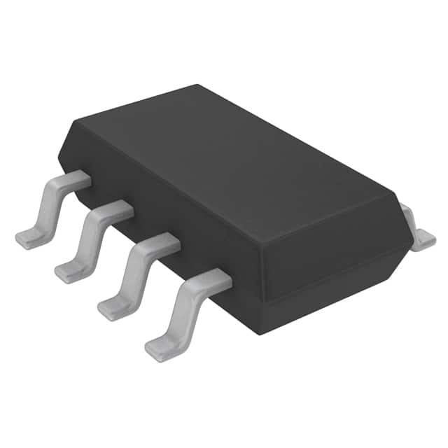
- Package: 8-Lead ThinSOT
- Essence: Converts digital signals into analog voltages
- Packaging/Quantity: Tape & Reel, 2500 units per reel
Specifications
- Resolution: 10 bits
- Output Type: Voltage
- Number of Channels: 1
- Supply Voltage Range: 2.7V to 5.5V
- Operating Temperature Range: -40°C to +85°C
- DNL (Differential Non-Linearity): ±0.5 LSB (max)
- INL (Integral Non-Linearity): ±1 LSB (max)
Pin Configuration
The LTC2640CTS8-HZ10#TRMPBF has the following pin configuration:
```
| | --| VDD GND |-- Power Supply --| REF AGND |-- Reference Voltage and Ground --| SDA SCL |-- I2C Serial Interface --| AOUT |-- Analog Output |___________| ```
Functional Features
- High precision DAC with 10-bit resolution
- Low noise output for accurate analog voltage generation
- I2C serial interface for easy communication with microcontrollers
- Wide supply voltage range allows for flexibility in different applications
- Small package size enables space-saving designs
Advantages
- High accuracy and resolution provide precise analog voltage outputs
- Low noise ensures minimal interference and improved signal quality
- I2C interface simplifies integration with other digital systems
- Wide supply voltage range allows for compatibility with various power sources
- Compact package size enables use in space-constrained applications
Disadvantages
- Limited to single-channel output, not suitable for multi-channel applications
- Requires external reference voltage for proper operation
- May be sensitive to noise and interference in the surrounding environment
Working Principles
The LTC2640CTS8-HZ10#TRMPBF is a digital-to-analog converter that converts digital signals into analog voltages. It utilizes a 10-bit resolution to provide high precision outputs. The device operates by receiving digital input data through the I2C serial interface. This data is then converted into an analog voltage output, which can be used in various applications such as control systems, instrumentation, and communication devices.
Detailed Application Field Plans
The LTC2640CTS8-HZ10#TRMPBF can be used in a wide range of applications, including:
- Industrial Control Systems: Providing accurate analog voltage references for precise control of industrial processes.
- Test and Measurement Equipment: Generating stable and precise analog signals for testing and calibration purposes.
- Audio Equipment: Producing high-quality audio signals with low noise and distortion.
- Communication Systems: Generating analog voltages for modulation and demodulation processes.
- Medical Devices: Providing precise analog voltage outputs for medical equipment such as patient monitors and diagnostic instruments.
Detailed and Complete Alternative Models
- LTC2640CTS8-HZ12#TRMPBF: Similar to LTC2640CTS8-HZ10#TRMPBF but with 12-bit resolution.
- LTC2640CTS8-HZ8#TRMPBF: Similar to LTC2640CTS8-HZ10#TRMPBF but with 8-bit resolution.
- LTC2640CTS8-HZ10#PBF: Through-hole package version of LTC2640CTS8-HZ10#TRMPBF.
(Note: This list is not exhaustive and there may be other alternative models available in the market.)
Word count: 409 words
10个与LTC2640CTS8-HZ10#TRMPBF在技术解决方案中的应用相关的常见问题及解答
Sure! Here are 10 common questions and answers related to the application of LTC2640CTS8-HZ10#TRMPBF in technical solutions:
Q: What is LTC2640CTS8-HZ10#TRMPBF? A: LTC2640CTS8-HZ10#TRMPBF is a high-precision, 10-bit digital-to-analog converter (DAC) manufactured by Linear Technology.
Q: What is the voltage range of LTC2640CTS8-HZ10#TRMPBF? A: The voltage range of LTC2640CTS8-HZ10#TRMPBF is 0V to VREF, where VREF is the reference voltage supplied to the DAC.
Q: How accurate is LTC2640CTS8-HZ10#TRMPBF? A: LTC2640CTS8-HZ10#TRMPBF has a typical integral nonlinearity (INL) of ±1 LSB and a maximum differential nonlinearity (DNL) of ±0.5 LSB, ensuring high accuracy.
Q: What is the power supply requirement for LTC2640CTS8-HZ10#TRMPBF? A: LTC2640CTS8-HZ10#TRMPBF requires a single power supply voltage ranging from 2.7V to 5.5V.
Q: Can LTC2640CTS8-HZ10#TRMPBF operate in both unipolar and bipolar modes? A: Yes, LTC2640CTS8-HZ10#TRMPBF can be configured to operate in either unipolar mode (0V to VREF) or bipolar mode (-VREF/2 to +VREF/2).
Q: What is the output settling time of LTC2640CTS8-HZ10#TRMPBF? A: LTC2640CTS8-HZ10#TRMPBF has a typical output settling time of 4.5μs, ensuring fast response in dynamic applications.
Q: Can LTC2640CTS8-HZ10#TRMPBF be controlled using a serial interface? A: Yes, LTC2640CTS8-HZ10#TRMPBF supports a 3-wire SPI-compatible serial interface for easy digital control.
Q: Does LTC2640CTS8-HZ10#TRMPBF have any internal reference voltage? A: No, LTC2640CTS8-HZ10#TRMPBF requires an external reference voltage (VREF) to set the output range.
Q: What is the temperature range of LTC2640CTS8-HZ10#TRMPBF? A: LTC2640CTS8-HZ10#TRMPBF operates over a temperature range of -40°C to +125°C, making it suitable for various environments.
Q: What are some typical applications of LTC2640CTS8-HZ10#TRMPBF? A: LTC2640CTS8-HZ10#TRMPBF is commonly used in precision instrumentation, industrial automation, and communication systems where accurate analog voltage generation is required.
Please note that the answers provided here are general and may vary depending on specific datasheet specifications and application requirements.