

LTC2640CTS8-LM10#TRMPBF
Product Overview
- Category: Integrated Circuit (IC)
- Use: Digital-to-Analog Converter (DAC)
- Characteristics: High precision, low noise, small package size
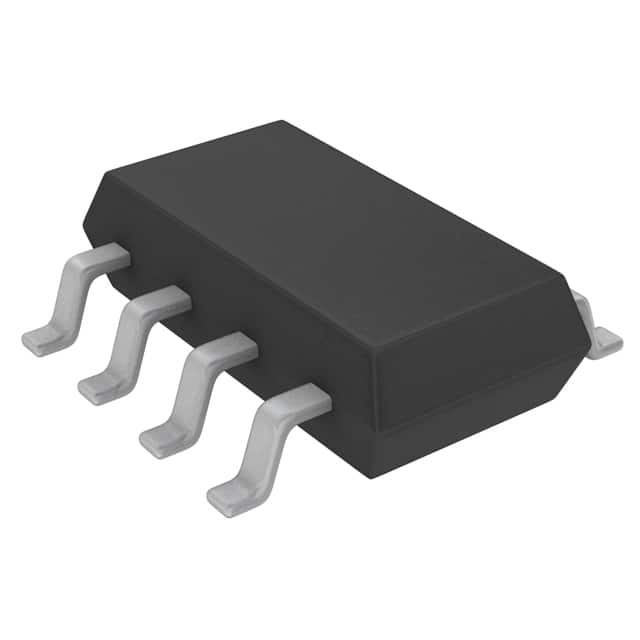
- Package: 8-Lead ThinSOT
- Essence: Converts digital signals into analog voltages
- Packaging/Quantity: Tape & Reel, 2500 units per reel
Specifications
- Resolution: 10 bits
- Number of Channels: 1
- Output Type: Voltage
- Output Range: 0V to VREF
- Reference Voltage Range: 2.5V to 5.5V
- Supply Voltage Range: 2.7V to 5.5V
- Operating Temperature Range: -40°C to +85°C
Pin Configuration
The LTC2640CTS8-LM10#TRMPBF has the following pin configuration:
- VIN - Input voltage
- GND - Ground
- SDA - Serial Data Input
- SCL - Serial Clock Input
- A0 - Address Input
- REF - Reference Voltage Input
- VOUT - Analog Voltage Output
- VCC - Supply Voltage
Functional Features
- High accuracy and resolution
- Low integral nonlinearity and offset error
- Low power consumption
- Fast settling time
- I2C compatible interface for easy communication with microcontrollers
Advantages
- Small package size allows for space-saving designs
- Wide operating temperature range enables usage in various environments
- Low noise output ensures high-quality analog signals
- Flexible reference voltage range accommodates different applications
Disadvantages
- Limited number of channels (only 1 channel)
- Requires an external reference voltage source
Working Principles
The LTC2640CTS8-LM10#TRMPBF is a digital-to-analog converter that converts digital signals into analog voltages. It utilizes an internal 10-bit DAC to accurately represent the digital input and generate the corresponding analog output voltage. The device operates using a supply voltage within the specified range and requires an external reference voltage for accurate conversion.
Detailed Application Field Plans
The LTC2640CTS8-LM10#TRMPBF can be used in various applications, including:
- Industrial automation: Control systems, process control, and instrumentation
- Test and measurement equipment: Signal generation, calibration, and data acquisition
- Audio equipment: Digital audio processing, volume control, and equalization
- Communication systems: Base stations, transceivers, and signal conditioning
- Automotive electronics: Infotainment systems, climate control, and driver assistance
Detailed and Complete Alternative Models
- LTC2640CMS8-LM10#PBF: Similar specifications but in a different package (8-Lead MSOP)
- LTC2640HTS8-LM10#TRMPBF: Higher temperature range (-40°C to +125°C) with the same specifications
- LTC2640ITS8-LM10#TRMPBF: Lower temperature range (-40°C to +70°C) with the same specifications
- LTC2640ZTS8-LM10#TRMPBF: Extended temperature range (-55°C to +125°C) with the same specifications
(Note: These alternative models are just examples and not an exhaustive list.)
This concludes the encyclopedia entry for LTC2640CTS8-LM10#TRMPBF, providing an overview of its product details, specifications, features, advantages, disadvantages, working principles, application field plans, and alternative models.
10个与LTC2640CTS8-LM10#TRMPBF在技术解决方案中的应用相关的常见问题及解答
Sure! Here are 10 common questions and answers related to the application of LTC2640CTS8-LM10#TRMPBF in technical solutions:
Q: What is the LTC2640CTS8-LM10#TRMPBF? A: The LTC2640CTS8-LM10#TRMPBF is a 10-bit voltage output digital-to-analog converter (DAC) manufactured by Linear Technology.
Q: What is the operating voltage range of LTC2640CTS8-LM10#TRMPBF? A: The operating voltage range of LTC2640CTS8-LM10#TRMPBF is from 2.7V to 5.5V.
Q: What is the resolution of LTC2640CTS8-LM10#TRMPBF? A: LTC2640CTS8-LM10#TRMPBF has a resolution of 10 bits, which means it can provide 1024 different output voltage levels.
Q: What is the typical output voltage range of LTC2640CTS8-LM10#TRMPBF? A: The typical output voltage range of LTC2640CTS8-LM10#TRMPBF is 0V to VREF, where VREF is the reference voltage supplied to the DAC.
Q: How can I interface with LTC2640CTS8-LM10#TRMPBF? A: LTC2640CTS8-LM10#TRMPBF can be interfaced using a standard serial peripheral interface (SPI) or I2C interface.
Q: What is the settling time of LTC2640CTS8-LM10#TRMPBF? A: The settling time of LTC2640CTS8-LM10#TRMPBF is typically 4.5μs, ensuring fast and accurate voltage output.
Q: Can LTC2640CTS8-LM10#TRMPBF operate in a low-power mode? A: Yes, LTC2640CTS8-LM10#TRMPBF has a low-power mode that reduces the power consumption when not actively changing the output voltage.
Q: What is the temperature range of LTC2640CTS8-LM10#TRMPBF? A: LTC2640CTS8-LM10#TRMPBF can operate within a temperature range of -40°C to +125°C.
Q: Does LTC2640CTS8-LM10#TRMPBF have any built-in reference voltage? A: No, LTC2640CTS8-LM10#TRMPBF requires an external reference voltage to set the output voltage range.
Q: What are some typical applications of LTC2640CTS8-LM10#TRMPBF? A: LTC2640CTS8-LM10#TRMPBF is commonly used in industrial automation, instrumentation, data acquisition systems, and other applications where precise analog voltage control is required.
Please note that the answers provided here are general and may vary depending on the specific datasheet and application requirements.