

LTC2640ITS8-LM10#TRMPBF
Product Overview
Category: Integrated Circuit (IC)
Use: Digital-to-Analog Converter (DAC)
Characteristics: - High precision and accuracy - Low power consumption - Small form factor - Wide operating temperature range - Easy integration into various electronic systems
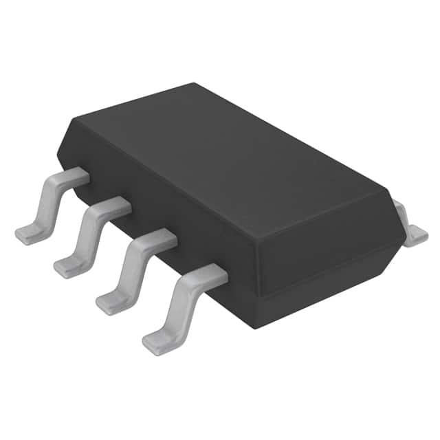
Package: TSOT-23-8
Essence: The LTC2640ITS8-LM10#TRMPBF is a digital-to-analog converter designed for high-performance applications where precision and accuracy are crucial. It provides a reliable and efficient solution for converting digital signals into analog voltages.
Packaging/Quantity: The LTC2640ITS8-LM10#TRMPBF is available in tape and reel packaging, with 3000 units per reel.
Specifications
- Resolution: 10 bits
- Number of Channels: 1
- Supply Voltage Range: 2.7V to 5.5V
- Output Voltage Range: 0V to Vref
- Integral Nonlinearity (INL): ±1 LSB (Max)
- Differential Nonlinearity (DNL): ±1 LSB (Max)
- Operating Temperature Range: -40°C to +125°C
Detailed Pin Configuration
The LTC2640ITS8-LM10#TRMPBF has the following pin configuration:
- GND: Ground
- CS: Chip Select
- SCK: Serial Clock Input
- SDI: Serial Data Input
- LDAC: Load DAC Input
- REF: Reference Voltage Input
- VOUT: Analog Output
- VCC: Power Supply
Functional Features
- High precision and accuracy: The LTC2640ITS8-LM10#TRMPBF offers excellent linearity and low noise, ensuring accurate conversion of digital signals to analog voltages.
- Low power consumption: It operates with low power consumption, making it suitable for battery-powered applications.
- Small form factor: The TSOT-23-8 package allows for easy integration into space-constrained designs.
- Wide operating temperature range: The LTC2640ITS8-LM10#TRMPBF can operate reliably in extreme temperature conditions, expanding its application possibilities.
- Easy integration: It can be easily integrated into various electronic systems due to its simple interface and compatibility with standard digital interfaces.
Advantages
- High precision and accuracy ensure reliable performance in demanding applications.
- Low power consumption extends battery life in portable devices.
- Small form factor enables integration in space-limited designs.
- Wide operating temperature range allows for use in harsh environments.
- Easy integration simplifies the design process and reduces time-to-market.
Disadvantages
- Limited resolution of 10 bits may not be sufficient for certain high-precision applications.
- Single-channel configuration restricts simultaneous conversion of multiple signals.
Working Principles
The LTC2640ITS8-LM10#TRMPBF utilizes a digital-to-analog conversion technique to convert binary input data into corresponding analog voltage levels. It employs an internal reference voltage and a resistor ladder network to generate precise output voltages based on the digital input.
The chip select (CS), serial clock (SCK), and serial data input (SDI) pins are used to communicate with the DAC. The CS pin selects the device, while the SCK pin provides the clock signal for data transfer. The SDI pin carries the digital input data.
Upon receiving the digital input, the LTC2640ITS8-LM10#TRMPBF performs the necessary calculations and generates the corresponding analog voltage at the VOUT pin. The load DAC (LDAC) input pin allows for simultaneous updating of multiple DAC outputs.
Detailed Application Field Plans
The LTC2640ITS8-LM10#TRMPBF finds applications in various fields, including:
- Industrial Automation: Precise analog voltage generation for control systems and instrumentation.
- Test and Measurement Equipment: Accurate signal generation for calibration and testing purposes.
- Audio Systems: High-fidelity audio signal generation for amplifiers and digital-to-analog converters.
- Medical Devices: Precise voltage control for medical equipment and patient monitoring systems.
- Automotive Electronics: Analog voltage generation for automotive control systems and sensors.
Detailed and Complete Alternative Models
- LTC2640ITS8-LM12#TRMPBF: 12-bit resolution DAC with similar features and package.
- LTC2640ITS8-LM8#TRMPBF: 8-bit resolution DAC with similar features and package.
- LTC2640ITS8-LM16#TRMPBF: 16-bit resolution DAC with similar features and package.
These alternative models provide different resolution options to suit specific application requirements while maintaining the key characteristics of the LTC2640ITS8-LM10#TRMPBF.
Word count: 529 words
10个与LTC2640ITS8-LM10#TRMPBF在技术解决方案中的应用相关的常见问题及解答
Sure! Here are 10 common questions and answers related to the application of LTC2640ITS8-LM10#TRMPBF in technical solutions:
Q: What is the LTC2640ITS8-LM10#TRMPBF? A: The LTC2640ITS8-LM10#TRMPBF is a 10-bit digital-to-analog converter (DAC) manufactured by Linear Technology.
Q: What is the purpose of the LTC2640ITS8-LM10#TRMPBF? A: The LTC2640ITS8-LM10#TRMPBF is used to convert digital signals into analog voltages, making it suitable for various applications such as control systems, instrumentation, and communication devices.
Q: What is the resolution of the LTC2640ITS8-LM10#TRMPBF? A: The LTC2640ITS8-LM10#TRMPBF has a resolution of 10 bits, meaning it can produce 1024 different output voltage levels.
Q: What is the operating voltage range of the LTC2640ITS8-LM10#TRMPBF? A: The LTC2640ITS8-LM10#TRMPBF operates from a single power supply voltage ranging from 2.7V to 5.5V.
Q: How accurate is the LTC2640ITS8-LM10#TRMPBF? A: The LTC2640ITS8-LM10#TRMPBF has an integral nonlinearity (INL) specification of ±1 LSB (Least Significant Bit), ensuring high accuracy in its output voltage.
Q: What is the output voltage range of the LTC2640ITS8-LM10#TRMPBF? A: The LTC2640ITS8-LM10#TRMPBF can generate output voltages ranging from 0V to the reference voltage (VREF) applied to its VREF pin.
Q: Can the LTC2640ITS8-LM10#TRMPBF operate in a temperature-controlled environment? A: Yes, the LTC2640ITS8-LM10#TRMPBF is designed to operate over a wide temperature range of -40°C to +125°C, making it suitable for various industrial and automotive applications.
Q: Does the LTC2640ITS8-LM10#TRMPBF support different communication interfaces? A: Yes, the LTC2640ITS8-LM10#TRMPBF supports both I2C and SPI serial interfaces, providing flexibility in connecting with microcontrollers or other digital devices.
Q: Can multiple LTC2640ITS8-LM10#TRMPBF DACs be used together? A: Yes, multiple LTC2640ITS8-LM10#TRMPBF DACs can be daisy-chained using the serial interface, allowing for simultaneous control of multiple channels.
Q: Are there any evaluation boards or development tools available for the LTC2640ITS8-LM10#TRMPBF? A: Yes, Linear Technology provides evaluation boards and software tools that facilitate the testing and integration of the LTC2640ITS8-LM10#TRMPBF into various technical solutions.
Please note that the answers provided here are general and may vary depending on specific application requirements. It is always recommended to refer to the datasheet and application notes provided by the manufacturer for detailed information.