

LTC6702CTS8#TRMPBF
Product Overview
- Category: Analog Comparator
- Use: The LTC6702CTS8#TRMPBF is used for comparing two analog voltage signals and providing a digital output based on the comparison result.
- Characteristics: It features low input offset voltage, low hysteresis, and high-speed operation.
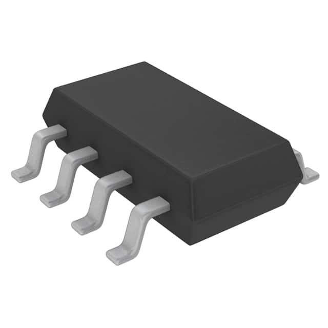
- Package: 8-Lead Thin SOT-23
- Essence: The LTC6702CTS8#TRMPBF is essential for applications requiring precise voltage comparisons.
- Packaging/Quantity: Available in tape and reel packaging with quantities specified by the manufacturer.
Specifications
- Input Offset Voltage: ±1mV
- Hysteresis: 3mV
- Response Time: 6ns
- Operating Temperature Range: -40°C to 85°C
- Supply Voltage Range: 2.7V to 11V
- Quiescent Current: 50µA
Detailed Pin Configuration
The LTC6702CTS8#TRMPBF has the following pin configuration: 1. IN+ 2. IN- 3. V- 4. GND 5. V+ 6. OUT 7. NC 8. REF
Functional Features
- High-Speed Comparator
- Low Input Offset Voltage
- Low Hysteresis
- Wide Supply Voltage Range
Advantages
- Precise voltage comparison
- High-speed operation
- Low power consumption
Disadvantages
- Limited operating temperature range
- Restricted supply voltage range
Working Principles
The LTC6702CTS8#TRMPBF operates by comparing the voltages present at the IN+ and IN- pins and providing a digital output based on the comparison result. It utilizes a high-speed comparator to achieve accurate and rapid voltage comparisons.
Detailed Application Field Plans
The LTC6702CTS8#TRMPBF is suitable for various applications including: - Precision voltage monitoring - Overvoltage/undervoltage detection - Signal conditioning circuits - Battery management systems
Detailed and Complete Alternative Models
Some alternative models to LTC6702CTS8#TRMPBF include: - LM311 - MAX902
In conclusion, the LTC6702CTS8#TRMPBF is a high-speed analog comparator with precise voltage comparison capabilities, making it suitable for a wide range of applications that require accurate voltage monitoring and signal conditioning.
Word count: 304
10个与LTC6702CTS8#TRMPBF在技术解决方案中的应用相关的常见问题及解答
What is the LTC6702CTS8#TRMPBF?
- The LTC6702CTS8#TRMPBF is a precision comparator with an adjustable hysteresis and a wide supply range, making it suitable for a variety of technical solutions.
What is the operating voltage range of LTC6702CTS8#TRMPBF?
- The LTC6702CTS8#TRMPBF has an operating voltage range from 2.7V to 36V, making it versatile for different power supply applications.
How can I adjust the hysteresis of LTC6702CTS8#TRMPBF?
- The hysteresis of LTC6702CTS8#TRMPBF can be adjusted using an external resistor, allowing for customization based on specific application requirements.
What are the typical applications of LTC6702CTS8#TRMPBF?
- Typical applications of LTC6702CTS8#TRMPBF include overvoltage/undervoltage protection, window comparators, level translators, and voltage monitoring circuits.
Does LTC6702CTS8#TRMPBF have built-in ESD protection?
- Yes, LTC6702CTS8#TRMPBF features built-in ESD protection, enhancing its reliability in harsh environments.
What is the input common-mode voltage range of LTC6702CTS8#TRMPBF?
- The input common-mode voltage range of LTC6702CTS8#TRMPBF extends from V- to V+ - 1.3V, accommodating various signal levels.
Can LTC6702CTS8#TRMPBF operate in high-temperature environments?
- Yes, LTC6702CTS8#TRMPBF is designed to operate reliably in high-temperature environments, with a temperature range of -40°C to 125°C.
Is LTC6702CTS8#TRMPBF suitable for battery-powered applications?
- Yes, LTC6702CTS8#TRMPBF's low quiescent current and wide supply range make it suitable for battery-powered applications, extending battery life.
What is the output drive capability of LTC6702CTS8#TRMPBF?
- LTC6702CTS8#TRMPBF has a rail-to-rail output stage with a sink current capability of 10mA, enabling direct interface with other components.
Are there any evaluation boards available for LTC6702CTS8#TRMPBF?
- Yes, there are evaluation boards available for LTC6702CTS8#TRMPBF, providing a convenient platform for testing and prototyping in technical solutions.