

P0900SDLRP Product Overview
Product Category
The P0900SDLRP belongs to the category of semiconductor devices.
Basic Information Overview
- Use: The P0900SDLRP is used as a voltage regulator in electronic circuits.
- Characteristics: It has high precision, low dropout voltage, and low quiescent current.
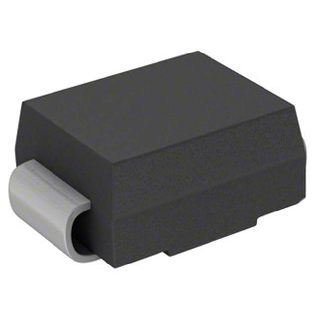
- Package: The P0900SDLRP is available in a small outline package (SOP) for surface mount applications.
- Essence: Its essence lies in providing stable and regulated voltage output.
- Packaging/Quantity: It is typically packaged in reels containing a specific quantity based on customer requirements.
Specifications
- Input Voltage Range: 2.5V to 6.5V
- Output Voltage Range: 1.2V to 5.5V
- Maximum Output Current: 500mA
- Dropout Voltage: 200mV at 100mA load
- Quiescent Current: 75µA
- Operating Temperature Range: -40°C to 85°C
Detailed Pin Configuration
The P0900SDLRP has a standard 5-pin configuration: 1. Input Voltage (VIN) 2. Ground (GND) 3. Enable (EN) 4. Bypass Capacitor (BYP) 5. Output Voltage (VOUT)
Functional Features
- Low Dropout Voltage: Ensures efficient regulation even with small input-output differentials.
- Low Quiescent Current: Minimizes power consumption in standby or idle modes.
- Thermal Shutdown Protection: Safeguards the device from overheating.
- Short Circuit Protection: Protects the device and the circuit from damage in case of a short circuit.
Advantages and Disadvantages
Advantages
- High precision voltage regulation
- Small form factor
- Low dropout voltage
- Low quiescent current
Disadvantages
- Limited maximum output current
- Restricted input voltage range
Working Principles
The P0900SDLRP utilizes a reference voltage and feedback mechanism to maintain a constant output voltage despite variations in input voltage and load conditions. It employs internal circuitry to regulate the output voltage and protect against fault conditions.
Detailed Application Field Plans
The P0900SDLRP is well-suited for various applications including: - Battery-powered devices - Portable consumer electronics - IoT devices - Wearable technology - Automotive electronics
Detailed and Complete Alternative Models
Some alternative models to the P0900SDLRP include: - P0800SDLRP: Lower output current but wider input voltage range - P1000SDLRP: Higher output current with similar characteristics - P1200SDLRP: Enhanced thermal performance for extreme temperature environments
In conclusion, the P0900SDLRP offers precise voltage regulation in a compact package, making it ideal for a wide range of electronic applications.
Word Count: 386
10个与P0900SDLRP在技术解决方案中的应用相关的常见问题及解答
What is P0900SDLRP?
- P0900SDLRP is a technical specification used in the design and development of electronic systems, particularly in the automotive industry.
How is P0900SDLRP applied in technical solutions?
- P0900SDLRP provides guidelines for the design, testing, and implementation of electronic control systems in vehicles, ensuring compatibility and reliability.
What are the key components of P0900SDLRP?
- The specification covers aspects such as hardware requirements, software interfaces, communication protocols, and diagnostic procedures for electronic systems.
Why is P0900SDLRP important in the automotive industry?
- P0900SDLRP helps standardize electronic system designs, leading to improved interoperability, safety, and performance in vehicles.
Are there any specific testing requirements outlined in P0900SDLRP?
- Yes, the specification includes testing procedures to validate the functionality and compliance of electronic control systems with P0900SDLRP standards.
How does P0900SDLRP impact vehicle maintenance and repair?
- By adhering to P0900SDLRP, technicians can accurately diagnose and address electronic system issues, leading to more efficient maintenance and repair processes.
Can P0900SDLRP be applied to non-automotive technical solutions?
- While primarily designed for automotive applications, the principles of P0900SDLRP can be adapted for use in other industries requiring robust electronic control systems.
Is P0900SDLRP a globally recognized standard?
- P0900SDLRP is widely recognized within the automotive industry and is often referenced by manufacturers, regulatory bodies, and technical professionals worldwide.
Does P0900SDLRP evolve over time to accommodate new technologies?
- Yes, the specification is periodically updated to incorporate advancements in electronic systems, ensuring its relevance in the rapidly changing automotive landscape.
Where can I find resources for implementing P0900SDLRP in technical solutions?
- Resources such as official documentation, training materials, and industry publications are available from relevant automotive associations and standards organizations.