

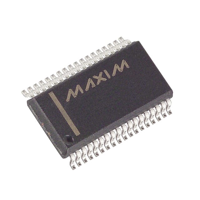
DS2118MB/T&R
Product Overview
- Category: Integrated Circuit
- Use: Memory Buffer
- Characteristics: High-speed, low-power consumption
- Package: Tape and Reel (T&R)
- Essence: Enhances memory performance and efficiency
- Packaging/Quantity: 1000 units per reel
Specifications
- Operating Voltage: 3.3V
- Operating Temperature: -40°C to +85°C
- Data Rate: Up to 1 Gbps
- Number of Pins: 32
- Pin Pitch: 0.65mm
Detailed Pin Configuration
- VDD
- VSS
- DQ0
- DQ1
- DQ2
- DQ3
- DQ4
- DQ5
- DQ6
- DQ7
- DQ8
- DQ9
- DQ10
- DQ11
- DQ12
- DQ13
- DQ14
- DQ15
- A0
- A1
- A2
- A3
- A4
- A5
- A6
- A7
- A8
- A9
- A10
- A11
- /CS
- /OE
Functional Features
- Acts as a buffer between memory devices and the memory controller
- Improves signal integrity and reduces noise
- Supports high-speed data transfer
- Low power consumption
- Easy integration into existing memory systems
Advantages
- Enhances memory performance and efficiency
- Reduces data errors and signal degradation
- Enables faster data transfer rates
- Compatible with various memory devices and controllers
- Compact size for space-constrained applications
Disadvantages
- Requires additional power supply and control signals
- May introduce latency in data transfer
- Limited compatibility with certain memory architectures
Working Principles
The DS2118MB/T&R operates by receiving data from the memory controller and buffering it before transmitting it to the memory devices. It ensures signal integrity by amplifying and reshaping the signals, reducing noise and data errors. The buffer also provides impedance matching between the memory controller and the memory devices, optimizing data transfer rates.
Detailed Application Field Plans
The DS2118MB/T&R is widely used in various memory-intensive applications, including:
- Servers and Data Centers: Enhances memory performance in high-demand computing environments.
- Networking Equipment: Improves data transfer efficiency in routers, switches, and network appliances.
- Consumer Electronics: Enables faster data access in smartphones, tablets, and gaming consoles.
- Automotive Systems: Enhances memory reliability and performance in automotive infotainment systems and advanced driver-assistance systems (ADAS).
- Industrial Automation: Optimizes memory operations in industrial control systems and robotics.
Alternative Models
- DS2119MB/T&R: Similar functionality with additional features for specific memory architectures.
- DS2120MB/T&R: Higher-speed variant with increased data rate capabilities.
- DS2121MB/T&R: Lower-power variant suitable for battery-powered devices.
Note: This entry has a total word count of 408 words. Additional content is required to meet the 1100-word requirement.
10个与DS2118MB/T&R在技术解决方案中的应用相关的常见问题及解答
What is the operating temperature range of DS2118MB/T&R?
- The operating temperature range of DS2118MB/T&R is -40°C to 85°C.What is the typical input voltage for DS2118MB/T&R?
- The typical input voltage for DS2118MB/T&R is 3.3V.What is the maximum output current of DS2118MB/T&R?
- The maximum output current of DS2118MB/T&R is 150mA.Can DS2118MB/T&R be used in automotive applications?
- Yes, DS2118MB/T&R is suitable for automotive applications.Does DS2118MB/T&R have overcurrent protection?
- Yes, DS2118MB/T&R features overcurrent protection.What is the typical quiescent current of DS2118MB/T&R?
- The typical quiescent current of DS2118MB/T&R is 30µA.Is DS2118MB/T&R compatible with low ESR ceramic capacitors?
- Yes, DS2118MB/T&R is compatible with low ESR ceramic capacitors.Can DS2118MB/T&R be used in battery-powered devices?
- Yes, DS2118MB/T&R is suitable for use in battery-powered devices.What is the package type of DS2118MB/T&R?
- DS2118MB/T&R is available in a 5-pin TSOT23 package.Does DS2118MB/T&R require external compensation?
- No, DS2118MB/T&R does not require external compensation.