

MAX5382LEUK+T
Product Overview
- Category: Digital-to-Analog Converter (DAC)
- Use: The MAX5382LEUK+T is a 10-bit voltage-output DAC designed for applications requiring high precision and low power consumption.
- Characteristics: It features a small package size, low power consumption, and high precision output.
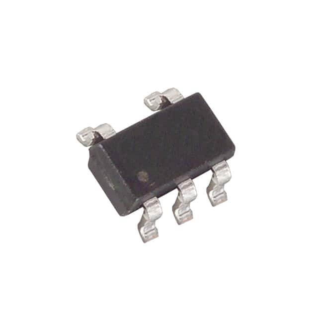
- Package: The MAX5382LEUK+T is available in a 3mm x 3mm, 10-pin µMAX package.
- Essence: This DAC provides a precise analog output voltage based on digital input signals.
- Packaging/Quantity: The MAX5382LEUK+T is typically available in reels of 2500 units.
Specifications
- Resolution: 10 bits
- Output Type: Voltage
- Package/Case: 10-µMAX
- Number of Channels: 1
- Settling Time: 6µs
- Operating Temperature Range: -40°C to +85°C
- Supply Voltage: 2.7V to 5.25V
- Power Consumption: 200µA (typical)
Detailed Pin Configuration
The MAX5382LEUK+T has the following pin configuration: 1. VDD: Power supply input 2. VOUT: Analog voltage output 3. GND: Ground 4. SCL: Serial clock input 5. SDA: Serial data input 6. A0: Address input 7. A1: Address input 8. LDAC: Load DAC input 9. CLR: Clear input 10. REF: Reference voltage input
Functional Features
- High precision output
- Low power consumption
- Small package size
- I2C-compatible interface
- Double-buffered input
Advantages and Disadvantages
Advantages
- High precision output
- Low power consumption
- Small package size
- Easy interfacing with microcontrollers
Disadvantages
- Limited output current capability
- Restricted temperature range compared to industrial-grade DACs
Working Principles
The MAX5382LEUK+T operates by converting digital input signals into a precise analog output voltage. It utilizes an internal reference voltage to generate the analog output, and its I2C-compatible interface allows for easy integration with microcontroller systems.
Detailed Application Field Plans
The MAX5382LEUK+T is well-suited for various applications including: - Precision instrumentation - Audio equipment - Industrial control systems - Test and measurement equipment - Data acquisition systems
Detailed and Complete Alternative Models
Some alternative models to the MAX5382LEUK+T include: - MAX5381LEUK+T: 8-bit voltage-output DAC - MAX5383LEUK+T: 12-bit voltage-output DAC - LTC1661CGN#PBF: 10-bit voltage-output DAC - AD5621BKSZ-500RL7: 12-bit voltage-output DAC
In conclusion, the MAX5382LEUK+T is a high-precision, low-power voltage-output DAC suitable for a wide range of applications that require accurate analog voltage generation.
Word count: 411
10个与MAX5382LEUK+T在技术解决方案中的应用相关的常见问题及解答
What is the MAX5382LEUK+T?
- The MAX5382LEUK+T is a 10-bit digital-to-analog converter (DAC) that can be used to convert digital signals into analog voltage outputs.
What is the operating voltage range of MAX5382LEUK+T?
- The operating voltage range of MAX5382LEUK+T is typically between 2.7V and 5.25V.
What is the resolution of MAX5382LEUK+T?
- MAX5382LEUK+T has a resolution of 10 bits, allowing for 1024 discrete voltage levels.
What are the typical applications of MAX5382LEUK+T?
- Typical applications of MAX5382LEUK+T include industrial process control, programmable gain amplifiers, and digitally controlled potentiometers.
How is MAX5382LEUK+T controlled?
- MAX5382LEUK+T is controlled through a serial interface using protocols such as I2C or SPI.
What is the output voltage range of MAX5382LEUK+T?
- The output voltage range of MAX5382LEUK+T is typically 0V to Vref, where Vref is the reference voltage.
Can MAX5382LEUK+T be used in automotive applications?
- Yes, MAX5382LEUK+T is suitable for use in automotive applications due to its wide operating voltage range and robust design.
What is the temperature range for MAX5382LEUK+T?
- MAX5382LEUK+T is designed to operate over a temperature range of -40°C to +125°C, making it suitable for harsh environments.
Does MAX5382LEUK+T have built-in non-volatile memory?
- No, MAX5382LEUK+T does not have built-in non-volatile memory, so external storage or backup may be required to retain settings across power cycles.
Is MAX5382LEUK+T available in a small form factor?
- Yes, MAX5382LEUK+T is available in a compact, space-saving package, making it suitable for applications with limited board space.