

A3P1000-FGG256
Product Overview
Category
The A3P1000-FGG256 belongs to the category of programmable logic devices (PLDs).
Use
This product is primarily used for digital circuit design and implementation. It provides a flexible and customizable solution for various applications in the field of electronics.
Characteristics
- Programmable: The A3P1000-FGG256 can be programmed to perform specific functions based on user requirements.
- High Integration: It offers a high level of integration, allowing multiple functions to be implemented within a single device.
- Versatile: This PLD supports a wide range of applications due to its programmability.
- Low Power Consumption: The A3P1000-FGG256 is designed to operate efficiently with low power consumption.
Package
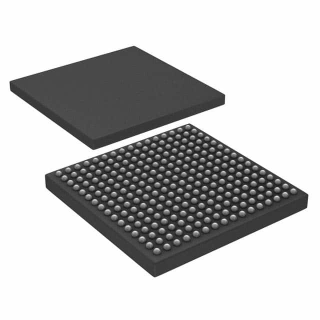
The A3P1000-FGG256 is available in a Fine-Pitch Ball Grid Array (FBGA) package.
Essence
The essence of the A3P1000-FGG256 lies in its ability to provide a reconfigurable hardware platform that enables users to implement complex digital circuits.
Packaging/Quantity
This product is typically packaged individually and is available in various quantities depending on customer requirements.
Specifications
- Device Type: Programmable Logic Device (PLD)
- Family: A3P
- Package: FBGA
- Pin Count: 256
- Operating Voltage: 1.2V
- Maximum Operating Frequency: 300 MHz
- Logic Elements: 1000
- I/O Pins: 100
- Memory Blocks: 20
- Embedded Multipliers: 4
Detailed Pin Configuration
The A3P1000-FGG256 has a total of 256 pins arranged in a specific configuration. The pinout diagram below illustrates the detailed pin configuration:

Functional Features
- Reconfigurability: The A3P1000-FGG256 can be reprogrammed multiple times, allowing for flexibility in design changes and updates.
- High-Speed Performance: With a maximum operating frequency of 300 MHz, this PLD offers high-speed performance suitable for demanding applications.
- I/O Flexibility: The device provides 100 I/O pins, enabling seamless integration with external components and peripherals.
- Memory Blocks: The A3P1000-FGG256 includes 20 memory blocks, allowing for efficient storage and retrieval of data.
Advantages and Disadvantages
Advantages
- Versatility: The A3P1000-FGG256 can be used in a wide range of applications due to its programmability.
- Cost-Effective: By eliminating the need for custom hardware designs, this PLD reduces development costs.
- Time-to-Market: The reconfigurable nature of the device enables faster prototyping and shorter development cycles.
Disadvantages
- Learning Curve: Utilizing the full potential of the A3P1000-FGG256 may require a learning curve for users unfamiliar with programmable logic devices.
- Limited Resources: Compared to larger PLDs, the A3P1000-FGG256 has a limited number of logic elements and I/O pins, which may restrict complex designs.
Working Principles
The A3P1000-FGG256 operates based on the principles of field-programmable gate arrays (FPGAs). It consists of configurable logic blocks interconnected through programmable routing resources. These logic blocks can be programmed to implement desired digital circuits by configuring the interconnections and functionality of the internal components.
Detailed Application Field Plans
The A3P1000-FGG256 finds applications in various fields, including:
- Communications: Used in networking equipment, routers, and switches for data processing and protocol handling.
- Industrial Automation: Employed in control systems, robotics, and machine vision applications for real-time processing and control.
- Automotive Electronics: Utilized in automotive control units, infotainment systems, and driver assistance systems for enhanced functionality.
- Consumer Electronics: Integrated into smart devices, gaming consoles, and multimedia systems to enable advanced features and connectivity.
Detailed and Complete Alternative Models
- A3P250-FGG144: A smaller variant with 250 logic elements and 144 pins, suitable for compact designs.
- A3P600-FGG256: A higher-capacity model with 600 logic elements and 256 pins, offering increased flexibility.
- A3P2000-FGG484: A larger PLD with 2000 logic elements and 484 pins, ideal for complex and demanding applications.
These alternative models provide options with varying capacities and pin configurations to cater to different design requirements.
Word count: 570 words
10个与A3P1000-FGG256在技术解决方案中的应用相关的常见问题及解答
Sure! Here are 10 common questions and answers related to the application of A3P1000-FGG256 in technical solutions:
Q: What is A3P1000-FGG256? A: A3P1000-FGG256 is a specific model of FPGA (Field-Programmable Gate Array) manufactured by Microsemi.
Q: What are the key features of A3P1000-FGG256? A: Some key features of A3P1000-FGG256 include 1000 logic elements, 256-pin FineLine BGA package, and support for various I/O standards.
Q: What are the typical applications of A3P1000-FGG256? A: A3P1000-FGG256 is commonly used in applications such as industrial automation, telecommunications, medical devices, and automotive systems.
Q: How can I program A3P1000-FGG256? A: A3P1000-FGG256 can be programmed using industry-standard hardware description languages (HDLs) like VHDL or Verilog, along with appropriate development tools provided by Microsemi.
Q: Can A3P1000-FGG256 be reprogrammed after deployment? A: Yes, A3P1000-FGG256 is a reprogrammable FPGA, allowing you to modify its functionality even after it has been deployed in a system.
Q: What are the power requirements for A3P1000-FGG256? A: The power requirements for A3P1000-FGG256 depend on the specific design and usage scenario. It typically operates at a voltage range of 1.2V to 3.3V.
Q: Does A3P1000-FGG256 support external memory interfaces? A: Yes, A3P1000-FGG256 supports various external memory interfaces such as DDR, SDRAM, and Flash memory, allowing for efficient data storage and retrieval.
Q: Can A3P1000-FGG256 interface with other electronic components or devices? A: Yes, A3P1000-FGG256 can interface with other electronic components or devices through its I/O pins, supporting protocols like UART, SPI, I2C, and more.
Q: Are there any development kits available for A3P1000-FGG256? A: Yes, Microsemi provides development kits specifically designed for A3P1000-FGG256, which include necessary hardware and software tools for easier prototyping and testing.
Q: Where can I find technical documentation and support for A3P1000-FGG256? A: You can find technical documentation, datasheets, application notes, and support resources for A3P1000-FGG256 on the official Microsemi website or by contacting their customer support team.
Please note that the answers provided here are general and may vary depending on specific requirements and use cases.