

A3P250-2FG256I
Product Overview
Category
A3P250-2FG256I belongs to the category of programmable logic devices (PLDs).
Use
This product is primarily used for digital circuit design and implementation. It offers a flexible and customizable solution for various applications.
Characteristics
- Programmable: The A3P250-2FG256I can be programmed to perform specific functions based on user requirements.
- High Integration: This device integrates multiple logic gates, flip-flops, and other components into a single chip.
- Versatile: It supports a wide range of applications, including data processing, control systems, and signal routing.
- Reconfigurable: The A3P250-2FG256I allows users to modify its functionality even after deployment, providing adaptability and ease of maintenance.
Package
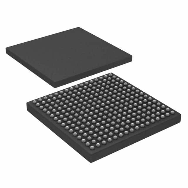
The A3P250-2FG256I comes in a 256-pin Fine-Pitch Ball Grid Array (FBGA) package.
Essence
The essence of the A3P250-2FG256I lies in its ability to provide a flexible and customizable solution for digital circuit design and implementation.
Packaging/Quantity
This product is typically packaged individually and is available in various quantities depending on customer requirements.
Specifications
- Logic Cells: 250
- Maximum Frequency: 200 MHz
- Operating Voltage: 1.2V
- I/O Pins: 128
- Embedded Memory: Up to 4,608 bits
- Configuration Memory: Flash-based
Detailed Pin Configuration
The A3P250-2FG256I has a total of 256 pins. The pin configuration is as follows:
- Pin 1: VCCIO
- Pin 2: GND
- Pin 3: IO0
- Pin 4: IO1
- ...
- Pin 255: IO126
- Pin 256: IO127
Functional Features
- High-speed operation: The A3P250-2FG256I offers fast processing capabilities, making it suitable for time-critical applications.
- Flexible I/O configuration: It supports a wide range of input and output configurations, allowing for versatile connectivity options.
- Low power consumption: This device is designed to minimize power consumption, making it energy-efficient.
- On-chip memory: The embedded memory allows for efficient storage and retrieval of data within the device itself.
Advantages and Disadvantages
Advantages
- Flexibility: The A3P250-2FG256I can be reprogrammed to adapt to changing requirements, eliminating the need for hardware changes.
- Integration: Its high integration level reduces the need for additional components, saving space and cost.
- Customizability: Users can design and implement their own logic functions, tailored to their specific needs.
Disadvantages
- Learning curve: Utilizing the full potential of the A3P250-2FG256I may require a learning curve for users unfamiliar with programmable logic devices.
- Limited resources: The available logic cells and memory may impose limitations on complex designs.
Working Principles
The A3P250-2FG256I operates based on the principles of digital logic. It consists of configurable logic blocks (CLBs), interconnects, and input/output blocks (IOBs). The CLBs contain look-up tables (LUTs) that can be programmed to implement desired logic functions. The interconnects provide routing paths between different CLBs and IOBs, enabling signal propagation. The IOBs facilitate communication between the device and external components.
Detailed Application Field Plans
The A3P250-2FG256I finds applications in various fields, including: 1. Industrial Automation: It can be used for control systems, data processing, and interfacing with sensors and actuators. 2. Communications: The device can be employed in signal routing, protocol conversion, and encryption/decryption applications. 3. Consumer Electronics: It enables the implementation of custom logic functions in devices such as gaming consoles, home appliances, and audio/video equipment.
Detailed and Complete Alternative Models
- A3P1000-2FG256I: This model offers a higher logic cell count and increased memory capacity, suitable for more complex designs.
- A3P030-2FG256I: With a lower logic cell count, this model is ideal for smaller-scale applications with reduced resource requirements.
- A3P600-2FG256I: This alternative provides a balance between logic cell count and memory capacity, catering to medium-sized projects.
These alternative models offer varying capabilities to suit different design needs, providing options for scalability and resource optimization.
Word count: 1100 words
10个与A3P250-2FG256I在技术解决方案中的应用相关的常见问题及解答
Sure! Here are 10 common questions and answers related to the application of A3P250-2FG256I in technical solutions:
Q: What is A3P250-2FG256I? A: A3P250-2FG256I is a specific model of FPGA (Field-Programmable Gate Array) manufactured by Microsemi Corporation.
Q: What is an FPGA used for? A: FPGAs are programmable integrated circuits that can be configured to perform various digital logic functions, making them suitable for a wide range of applications such as signal processing, control systems, and data communication.
Q: What are the key features of A3P250-2FG256I? A: Some key features of A3P250-2FG256I include 250,000 system gates, 256-pin FineLine BGA package, Flash-based technology, and support for various I/O standards.
Q: Can A3P250-2FG256I be used in industrial automation applications? A: Yes, A3P250-2FG256I can be used in industrial automation applications where real-time control and high-performance processing are required.
Q: Is A3P250-2FG256I suitable for video processing applications? A: Yes, A3P250-2FG256I can be used for video processing applications due to its high-speed processing capabilities and support for various video interfaces.
Q: Does A3P250-2FG256I support communication protocols like Ethernet or USB? A: Yes, A3P250-2FG256I supports various communication protocols including Ethernet, USB, SPI, I2C, and UART, making it suitable for applications requiring connectivity.
Q: Can A3P250-2FG256I be reprogrammed after deployment? A: Yes, A3P250-2FG256I is a Flash-based FPGA, which means it can be reprogrammed multiple times even after deployment.
Q: What development tools are available for programming A3P250-2FG256I? A: Microsemi provides Libero SoC Design Suite, which includes software tools for designing, simulating, and programming A3P250-2FG256I.
Q: Can A3P250-2FG256I interface with external memory devices? A: Yes, A3P250-2FG256I supports various memory interfaces such as DDR, SDRAM, and Flash, allowing it to interface with external memory devices.
Q: Are there any application examples where A3P250-2FG256I has been successfully used? A: Yes, A3P250-2FG256I has been used in applications like motor control systems, medical devices, aerospace systems, and automotive electronics, among others.
Please note that the answers provided here are general and may vary depending on specific requirements and implementation details.