

A3P250-2FGG256
Product Overview
Category
A3P250-2FGG256 belongs to the category of Field Programmable Gate Arrays (FPGAs).
Use
This product is primarily used in digital logic circuits for various applications such as telecommunications, automotive, industrial automation, and consumer electronics.
Characteristics
- High-performance programmable logic device
- Offers flexibility and reconfigurability
- Provides fast prototyping and development capabilities
- Supports complex digital designs
- Low power consumption
- High-speed data processing
Package
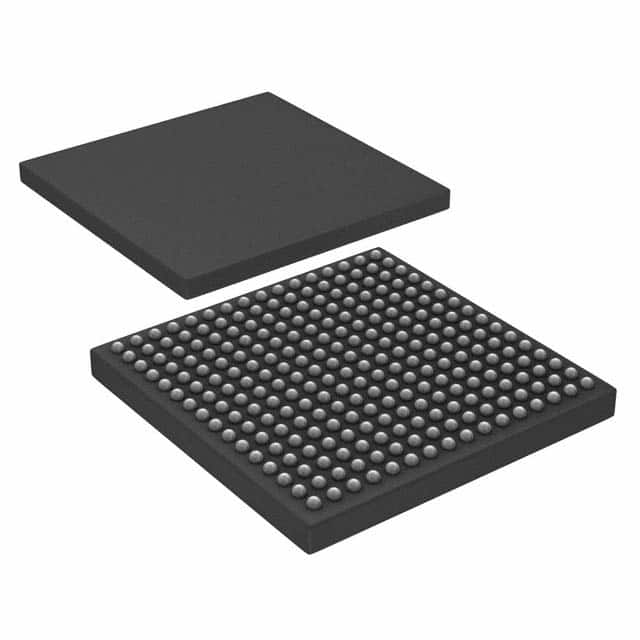
A3P250-2FGG256 comes in a 256-ball Fine-Pitch Ball Grid Array (FBGA) package.
Essence
The essence of this product lies in its ability to provide a customizable and versatile solution for implementing complex digital logic circuits.
Packaging/Quantity
Each package contains one A3P250-2FGG256 FPGA.
Specifications
- Logic Elements: 250,000
- Embedded Memory: 1,536 Kbits
- Maximum User I/Os: 232
- Clock Management Tiles: 8
- DSP Blocks: 96
- Maximum Operating Frequency: 400 MHz
- Operating Voltage: 1.2V
- Package Type: FBGA
- Package Pins: 256
- Temperature Range: -40°C to +100°C
Detailed Pin Configuration
For a detailed pin configuration diagram of A3P250-2FGG256, please refer to the manufacturer's datasheet or documentation.
Functional Features
- Configurable logic blocks for implementing custom digital circuits
- Dedicated clock management tiles for precise timing control
- Built-in DSP blocks for efficient signal processing
- Flexible I/O interfaces for seamless integration with external devices
- On-chip memory resources for data storage and retrieval
- Support for various communication protocols and standards
Advantages and Disadvantages
Advantages
- High flexibility and reconfigurability
- Fast prototyping and development capabilities
- Low power consumption
- High-speed data processing
- Wide range of applications
Disadvantages
- Steeper learning curve compared to traditional fixed-function integrated circuits
- Higher cost compared to standard logic gates or microcontrollers for simple applications
Working Principles
A3P250-2FGG256 is based on the principle of field programmability, where the internal logic elements can be configured and interconnected to implement desired digital circuits. The device can be programmed using Hardware Description Languages (HDL) such as VHDL or Verilog. Once programmed, the FPGA executes the desired logic operations based on the input signals received.
Detailed Application Field Plans
A3P250-2FGG256 finds extensive application in various fields, including:
- Telecommunications: Used in network routers, switches, and communication equipment for high-speed data processing and protocol handling.
- Automotive: Employed in automotive electronics for control systems, driver assistance, and infotainment applications.
- Industrial Automation: Utilized in programmable logic controllers (PLCs), motor control systems, and industrial monitoring devices.
- Consumer Electronics: Integrated into smart TVs, gaming consoles, and multimedia devices for enhanced functionality and performance.
Detailed and Complete Alternative Models
- A3P1000-FGG144: Offers higher logic capacity and more I/O pins for larger-scale designs.
- A3P060-VQG100: Provides a smaller form factor with lower logic capacity suitable for compact applications.
- A3P030-TQG100: Entry-level FPGA with limited resources, ideal for simple digital circuit implementations.
Please note that the above list is not exhaustive, and there are several other alternative models available from the manufacturer.
Word count: 550 words
10个与A3P250-2FGG256在技术解决方案中的应用相关的常见问题及解答
Sure! Here are 10 common questions and answers related to the application of A3P250-2FGG256 in technical solutions:
Q: What is A3P250-2FGG256? A: A3P250-2FGG256 is a specific model of FPGA (Field-Programmable Gate Array) manufactured by Microsemi.
Q: What is an FPGA used for? A: FPGAs are programmable integrated circuits that can be configured to perform various functions, such as digital signal processing, data encryption, and control logic implementation.
Q: What are the key features of A3P250-2FGG256? A: Some key features of A3P250-2FGG256 include 250,000 system gates, 256-pin FineLine BGA package, and Flash-based technology for non-volatile configuration storage.
Q: What applications can benefit from using A3P250-2FGG256? A: A3P250-2FGG256 can be used in a wide range of applications, including industrial automation, telecommunications, automotive electronics, medical devices, and aerospace systems.
Q: How do I program the A3P250-2FGG256 FPGA? A: The A3P250-2FGG256 FPGA can be programmed using design software provided by Microsemi, such as Libero SoC or Designer.
Q: Can I reprogram the A3P250-2FGG256 after it has been deployed in a system? A: Yes, the A3P250-2FGG256 FPGA is reprogrammable, allowing you to update or modify its functionality even after it has been installed in a system.
Q: What development tools are available for designing with A3P250-2FGG256? A: Microsemi provides a range of development tools, including design software, evaluation boards, reference designs, and technical documentation to assist in the design process.
Q: What is the power consumption of A3P250-2FGG256? A: The power consumption of A3P250-2FGG256 depends on the specific design and configuration. It is recommended to refer to the datasheet or consult Microsemi's technical support for detailed power specifications.
Q: Can I interface A3P250-2FGG256 with other components or peripherals? A: Yes, A3P250-2FGG256 supports various communication interfaces such as SPI, I2C, UART, and GPIOs, allowing it to interface with other components or peripherals in your system.
Q: Where can I find additional resources and support for A3P250-2FGG256? A: Microsemi's website provides comprehensive documentation, application notes, and technical support forums where you can find additional resources and get assistance with A3P250-2FGG256.