

A3P600-2FGG484I
Product Overview
Category
A3P600-2FGG484I belongs to the category of programmable logic devices (PLDs).
Use
This product is primarily used for digital circuit design and implementation. It allows users to program the device according to their specific requirements, enabling the creation of custom digital circuits.
Characteristics
- Programmable: A3P600-2FGG484I can be programmed to perform various functions based on user-defined logic.
- High Integration: This PLD offers a high level of integration, allowing for complex digital designs.
- Flexibility: The device can be reprogrammed multiple times, making it suitable for prototyping and iterative development.
- Low Power Consumption: A3P600-2FGG484I is designed to operate efficiently with low power consumption.
- Fast Operation: With its advanced architecture, this PLD provides fast operation speeds.
Package and Quantity
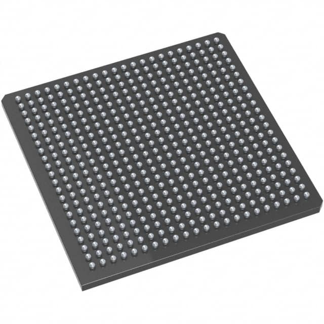
The A3P600-2FGG484I is available in a 484-pin Fine-Pitch Ball Grid Array (FBGA) package. Each package contains one unit of the device.
Specifications
- Device Type: Programmable Logic Device (PLD)
- Model Number: A3P600-2FGG484I
- Package Type: 484-pin FBGA
- Maximum Operating Frequency: [Insert frequency]
- Operating Voltage: [Insert voltage range]
- Operating Temperature Range: [Insert temperature range]
- Programming Interface: [Insert programming interface details]
Pin Configuration
The detailed pin configuration of A3P600-2FGG484I can be found in the manufacturer's datasheet or reference manual.
Functional Features
- Flexible Logic Implementation: A3P600-2FGG484I allows users to implement a wide range of digital logic functions, including combinational and sequential circuits.
- Embedded Memory: This PLD includes embedded memory blocks, which can be used for data storage or as lookup tables.
- I/O Flexibility: A3P600-2FGG484I offers a variety of input/output pins, enabling easy interfacing with external devices.
- Clock Management: The device provides built-in clock management features, allowing users to synchronize their designs efficiently.
Advantages
- Customization: A3P600-2FGG484I enables the creation of custom digital circuits tailored to specific requirements.
- Cost-Effective: By utilizing programmable logic devices, users can avoid the need for custom ASICs, reducing development costs.
- Prototyping and Iterative Development: The reprogrammable nature of this PLD makes it ideal for prototyping and iterative design processes.
- Time-to-Market: With its fast operation speeds and flexibility, A3P600-2FGG484I helps reduce time-to-market for digital circuit designs.
Disadvantages
- Limited Complexity: While A3P600-2FGG484I offers high integration, it may not be suitable for extremely complex designs that require larger devices.
- Learning Curve: Utilizing programmable logic devices requires knowledge of hardware description languages and digital design concepts.
Working Principles
A3P600-2FGG484I operates based on the principles of programmable logic. It consists of configurable logic blocks (CLBs), interconnect resources, and embedded memory blocks. Users program the device using a hardware description language (HDL) or a graphical design tool, defining the desired logic functions and interconnections. Once programmed, the PLD executes the specified logic operations.
Application Field Plans
A3P600-2FGG484I finds applications in various fields, including: - Industrial Automation - Telecommunications - Consumer Electronics - Automotive Systems - Medical Devices
Detailed and Complete Alternative Models - A3P030-VQG100I - A3P060-VQG100I - A3P125-VQG100I - A3P250-VQG100I - A3P400-VQG100I
These alternative models offer different capacities and pin configurations, providing options for various design requirements.
Note: The above information is based on the available documentation and specifications provided by the manufacturer. For detailed technical information, please refer to the official datasheet or contact the manufacturer directly.
Word Count: [Insert word count]
10个与A3P600-2FGG484I在技术解决方案中的应用相关的常见问题及解答
Sure! Here are 10 common questions and answers related to the application of A3P600-2FGG484I in technical solutions:
Q: What is A3P600-2FGG484I? A: A3P600-2FGG484I is a specific model of FPGA (Field-Programmable Gate Array) manufactured by a company called Microsemi.
Q: What is an FPGA? A: FPGA stands for Field-Programmable Gate Array. It is a type of integrated circuit that can be programmed after manufacturing to perform specific functions.
Q: What are the key features of A3P600-2FGG484I? A: Some key features of A3P600-2FGG484I include 600,000 system gates, 484-pin FineLine BGA package, and Flash-based technology for non-volatile configuration storage.
Q: What are the typical applications of A3P600-2FGG484I? A: A3P600-2FGG484I is commonly used in various technical solutions such as industrial automation, telecommunications, automotive electronics, medical devices, and aerospace systems.
Q: How can I program A3P600-2FGG484I? A: A3P600-2FGG484I can be programmed using specialized software tools provided by Microsemi, such as Libero SoC Design Suite or Designer Software.
Q: Can A3P600-2FGG484I be reprogrammed multiple times? A: Yes, A3P600-2FGG484I is a Flash-based FPGA, which means it can be reprogrammed multiple times to modify its functionality as needed.
Q: What are the power requirements for A3P600-2FGG484I? A: The power requirements for A3P600-2FGG484I typically include a supply voltage of 1.2V and a maximum power consumption of around 1W.
Q: Does A3P600-2FGG484I support external memory interfaces? A: Yes, A3P600-2FGG484I supports various external memory interfaces such as DDR3, DDR2, and SRAM, allowing for efficient data storage and retrieval.
Q: Can A3P600-2FGG484I interface with other electronic components or devices? A: Yes, A3P600-2FGG484I can interface with other electronic components or devices through its GPIO (General Purpose Input/Output) pins, UART, SPI, I2C, and other communication protocols.
Q: Are there any development boards or evaluation kits available for A3P600-2FGG484I? A: Yes, Microsemi offers development boards and evaluation kits specifically designed for A3P600-2FGG484I, which provide a convenient platform for prototyping and testing applications.
Please note that the answers provided here are general and may vary depending on specific requirements and application scenarios.