

A3PE1500-2FGG676I
Product Overview
Category
The A3PE1500-2FGG676I belongs to the category of programmable logic devices (PLDs).
Use
This product is primarily used in digital circuit design and implementation. It provides a flexible and customizable solution for various applications.
Characteristics
- Programmable: The A3PE1500-2FGG676I can be programmed to perform specific functions based on the user's requirements.
- High-performance: It offers fast processing speeds and efficient execution of complex tasks.
- Versatile: This PLD supports a wide range of applications, making it suitable for diverse industries.
- Compact package: The A3PE1500-2FGG676I comes in a compact form factor, allowing for easy integration into different systems.
- Reliable: It ensures stable and reliable operation even under demanding conditions.
Package and Quantity
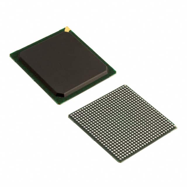
The A3PE1500-2FGG676I is packaged in a 676-pin Fine-Pitch Ball Grid Array (FBGA) package. Each package contains one unit of the PLD.
Specifications
- Device Type: Programmable Logic Device (PLD)
- Family: A3P
- Series: E1500
- Model: 2FGG676I
- Number of Pins: 676
- Package Type: FBGA
- Operating Voltage: 1.2V
- Maximum Operating Frequency: 500 MHz
- Logic Cells: 1,500
- I/O Banks: 8
- Embedded Memory: 4,000 Kbits
- Configuration Method: JTAG, AS, or SPI
Detailed Pin Configuration
The A3PE1500-2FGG676I has a total of 676 pins, which are organized into various functional groups. The pin configuration is as follows:
- Pin Group 1: Power Supply (VCC, GND)
- Pin Group 2: Configuration Interface (JTAG, AS, SPI)
- Pin Group 3: Input/Output Banks (IOB)
- Pin Group 4: Clock Inputs (CLK)
- Pin Group 5: Special Function Pins (RESET, TEST)
- Pin Group 6: Embedded Memory Interface (MEM)
- Pin Group 7: Miscellaneous Control Signals (CTRL)
- Pin Group 8: Reserved Pins
For a detailed pin configuration diagram, please refer to the product datasheet.
Functional Features
The A3PE1500-2FGG676I offers several functional features that enhance its performance and usability. These include:
- High-speed operation: The PLD supports fast data processing and execution of complex algorithms.
- Flexible I/O configuration: It allows for versatile input/output configurations, enabling seamless integration with external devices.
- Embedded memory: The A3PE1500-2FGG676I includes a significant amount of embedded memory, facilitating efficient data storage and retrieval.
- Clock management: The PLD provides various clocking options, allowing precise synchronization of internal operations.
- Design security: It incorporates security features to protect intellectual property and prevent unauthorized access to the design.
Advantages and Disadvantages
Advantages
- Versatile and customizable solution for digital circuit design.
- High-performance capabilities enable efficient execution of complex tasks.
- Compact form factor facilitates easy integration into different systems.
- Reliable operation ensures stable performance under demanding conditions.
- Offers design security features to protect intellectual property.
Disadvantages
- Requires expertise in digital circuit design and programming.
- Limited availability of alternative models from other manufacturers.
- Higher cost compared to standard off-the-shelf integrated circuits.
Working Principles
The A3PE1500-2FGG676I operates based on the principles of programmable logic. It consists of a matrix of configurable logic blocks (CLBs) interconnected through programmable interconnects. The device can be programmed using hardware description languages (HDL) or design entry tools to define the desired functionality.
Upon programming, the PLD's internal configuration memory stores the user-defined logic functions and interconnections. During operation, input signals are processed through the configured logic elements, producing the desired output based on the programmed functionality.
Detailed Application Field Plans
The A3PE1500-2FGG676I finds applications in various fields, including:
- Telecommunications: Used in network routers, switches, and communication equipment for high-speed data processing.
- Industrial Automation: Employed in control systems, robotics, and factory automation for real-time data processing and control.
- Automotive Electronics: Integrated into automotive control units, infotainment systems, and driver assistance systems for enhanced performance and functionality.
- Aerospace and Defense: Utilized in avionics, radar systems, and military-grade electronics for reliable and high-performance operation.
- Medical Devices: Incorporated into medical imaging equipment, patient monitoring systems, and diagnostic
10个与A3PE1500-2FGG676I在技术解决方案中的应用相关的常见问题及解答
Sure! Here are 10 common questions and answers related to the application of A3PE1500-2FGG676I in technical solutions:
Q: What is the A3PE1500-2FGG676I? A: The A3PE1500-2FGG676I is a field-programmable gate array (FPGA) manufactured by Microsemi Corporation.
Q: What are the key features of the A3PE1500-2FGG676I? A: Some key features include 1.5 million system gates, 1.8V core voltage, 676-pin FineLine BGA package, and support for various I/O standards.
Q: What are the typical applications of the A3PE1500-2FGG676I? A: The A3PE1500-2FGG676I is commonly used in applications such as telecommunications, industrial automation, medical devices, aerospace, and defense.
Q: How can I program the A3PE1500-2FGG676I? A: The A3PE1500-2FGG676I can be programmed using industry-standard hardware description languages (HDLs) like VHDL or Verilog, along with appropriate development tools provided by Microsemi.
Q: What is the maximum operating frequency of the A3PE1500-2FGG676I? A: The maximum operating frequency of the A3PE1500-2FGG676I depends on the specific design and implementation, but it can typically reach frequencies in the hundreds of megahertz range.
Q: Can the A3PE1500-2FGG676I interface with other components or devices? A: Yes, the A3PE1500-2FGG676I supports various I/O standards, allowing it to interface with other components or devices such as memories, sensors, communication interfaces, and more.
Q: Does the A3PE1500-2FGG676I have built-in security features? A: Yes, the A3PE1500-2FGG676I offers built-in security features like bitstream encryption, tamper detection, and secure boot capabilities to protect against unauthorized access or IP theft.
Q: Can the A3PE1500-2FGG676I be used in safety-critical applications? A: Yes, the A3PE1500-2FGG676I can be used in safety-critical applications, provided that appropriate design methodologies and safety standards are followed during development.
Q: What is the power consumption of the A3PE1500-2FGG676I? A: The power consumption of the A3PE1500-2FGG676I depends on the specific design and utilization, but it typically operates within a range of a few watts.
Q: Are there any evaluation boards or development kits available for the A3PE1500-2FGG676I? A: Yes, Microsemi provides evaluation boards and development kits specifically designed for the A3PE1500-2FGG676I, which include necessary hardware and software tools for prototyping and development.
Please note that the answers provided here are general and may vary depending on specific requirements and use cases. It's always recommended to refer to the official documentation and datasheets for accurate and up-to-date information.