

A3PN060-1VQ100
Product Overview
Category
A3PN060-1VQ100 belongs to the category of programmable logic devices (PLDs).
Use
This product is commonly used in digital circuit design and implementation. It provides a flexible and customizable solution for various applications.
Characteristics
- Programmable: The A3PN060-1VQ100 can be programmed to perform specific functions based on the user's requirements.
- Versatile: It supports a wide range of applications, including data processing, control systems, and communication protocols.
- High-performance: The device offers fast processing speeds and efficient utilization of resources.
- Low power consumption: It is designed to minimize power usage, making it suitable for battery-powered devices.
- Compact package: The A3PN060-1VQ100 is available in a small form factor, allowing for space-efficient integration into electronic systems.
Package and Quantity
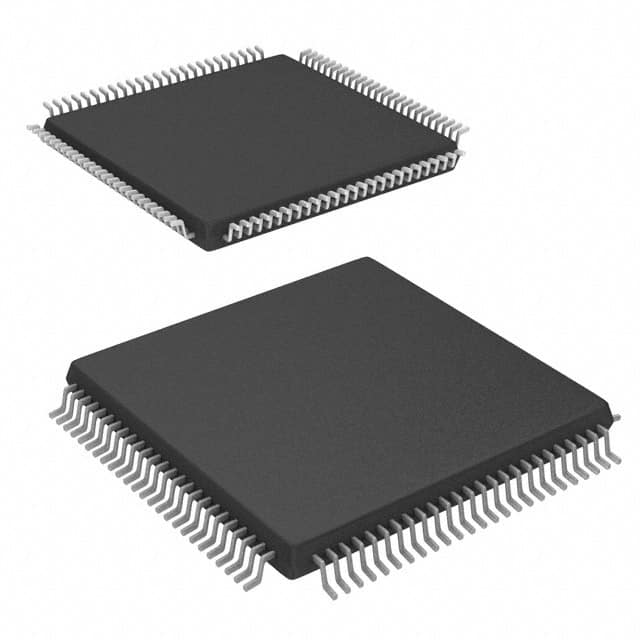
The A3PN060-1VQ100 is typically packaged in a quad flat pack (QFP) with 100 pins. Each package contains one unit of the device.
Specifications
- Device Model: A3PN060-1VQ100
- Logic Elements: 60,000
- Flip-Flops: 2,560
- Maximum Frequency: 250 MHz
- I/O Pins: 96
- Operating Voltage: 3.3V
- Package Type: Quad Flat Pack (QFP)
- Package Pins: 100
Pin Configuration
The pin configuration of the A3PN060-1VQ100 is as follows:
[Insert detailed pin configuration diagram here]
Functional Features
- High-speed operation: The A3PN060-1VQ100 offers fast processing capabilities, enabling efficient execution of complex algorithms.
- Flexible I/O options: It provides a sufficient number of I/O pins for interfacing with external devices and peripherals.
- On-chip memory: The device includes embedded memory blocks, allowing for efficient storage and retrieval of data.
- Design reusability: The A3PN060-1VQ100 supports the use of pre-designed intellectual property (IP) cores, enabling faster development cycles.
Advantages and Disadvantages
Advantages
- Customizability: The programmable nature of the A3PN060-1VQ100 allows for tailored solutions to specific application requirements.
- Cost-effective: By eliminating the need for dedicated hardware components, it reduces overall system costs.
- Time-saving: The device enables rapid prototyping and iterative design improvements without requiring extensive hardware modifications.
Disadvantages
- Learning curve: Utilizing the full potential of the A3PN060-1VQ100 may require a learning period for users unfamiliar with programmable logic devices.
- Limited resources: The device has a finite number of logic elements and I/O pins, which may restrict the complexity of designs that can be implemented.
Working Principles
The A3PN060-1VQ100 operates based on the principles of field-programmable gate arrays (FPGAs). It consists of an array of configurable logic blocks interconnected through programmable routing resources. These logic blocks can be programmed to perform various functions, such as logic operations, arithmetic calculations, and memory storage. The configuration of the device is stored in non-volatile memory, allowing it to retain its programmed functionality even after power cycles.
Application Field Plans
The A3PN060-1VQ100 finds applications in various fields, including:
- Embedded Systems: It can be used to implement control systems, interface protocols, and data processing units in embedded devices.
- Communication Systems: The device enables the development of custom communication protocols and signal processing algorithms.
- Industrial Automation: It can be utilized for implementing control logic in industrial automation systems, such as robotics and process control.
- Automotive Electronics: The A3PN060-1VQ100 can be employed in automotive applications, including engine management systems and driver assistance systems.
Alternative Models
Here are some alternative models that offer similar functionality:
- A3P250-VQG100
- A3P600-PQG208
- A3P1000-FG144
These models provide varying capacities and pin configurations to cater to different project requirements.
In conclusion, the A3PN060-1VQ100 is a versatile programmable logic device with high-performance capabilities. Its customizable nature, compact package, and wide range of applications make it a valuable component in digital circuit design and implementation.
10个与A3PN060-1VQ100在技术解决方案中的应用相关的常见问题及解答
Sure! Here are 10 common questions and answers related to the application of A3PN060-1VQ100 in technical solutions:
1. What is A3PN060-1VQ100? - A3PN060-1VQ100 is a specific model number of a field-programmable gate array (FPGA) manufactured by Microsemi Corporation.
2. What are the key features of A3PN060-1VQ100? - Some key features of A3PN060-1VQ100 include 60,000 system gates, 1,152 logic elements, 64 macrocells, and 32 I/O pins.
3. What is the typical application of A3PN060-1VQ100? - A3PN060-1VQ100 is commonly used in various technical solutions such as industrial automation, telecommunications, automotive electronics, and medical devices.
4. How can A3PN060-1VQ100 be programmed? - A3PN060-1VQ100 can be programmed using hardware description languages (HDLs) like VHDL or Verilog, or through graphical programming tools provided by the manufacturer.
5. Can A3PN060-1VQ100 be reprogrammed after initial programming? - Yes, A3PN060-1VQ100 is a reprogrammable FPGA, which means it can be reprogrammed multiple times to implement different functionalities.
6. What are the power requirements for A3PN060-1VQ100? - A3PN060-1VQ100 typically operates at a voltage range of 3.0V to 3.6V and requires a stable power supply with appropriate current capabilities.
7. Does A3PN060-1VQ100 support external memory interfaces? - Yes, A3PN060-1VQ100 supports various external memory interfaces such as synchronous dynamic random-access memory (SDRAM) and flash memory.
8. Can A3PN060-1VQ100 interface with other digital components or microcontrollers? - Yes, A3PN060-1VQ100 can interface with other digital components or microcontrollers through standard communication protocols like SPI, I2C, UART, or GPIO pins.
9. What are the temperature operating limits for A3PN060-1VQ100? - A3PN060-1VQ100 typically operates within a temperature range of -40°C to +85°C, making it suitable for both industrial and commercial applications.
10. Are there any development tools available for A3PN060-1VQ100? - Yes, Microsemi provides development tools like Libero SoC Design Suite and SmartFusion Evaluation Kit that can be used for designing and programming A3PN060-1VQ100-based solutions.
Please note that the answers provided here are general and may vary depending on specific application requirements and manufacturer's documentation.