

A3PN060-1VQG100
Product Overview
Category
A3PN060-1VQG100 belongs to the category of programmable logic devices (PLDs).
Use
This product is commonly used in digital circuit design and implementation. It provides a flexible and customizable solution for various applications.
Characteristics
- Programmable: The A3PN060-1VQG100 can be programmed to perform specific functions based on user requirements.
- Versatile: It supports a wide range of applications due to its programmability.
- High-performance: The device offers fast processing speeds and efficient operation.
- Compact: The A3PN060-1VQG100 is designed to be small in size, making it suitable for space-constrained applications.
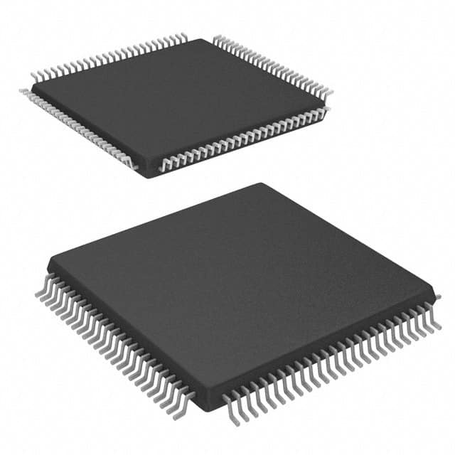
Package
The A3PN060-1VQG100 is typically available in a quad flat pack (QFP) package.
Essence
The essence of this product lies in its ability to provide reconfigurable logic functionality, allowing users to implement custom digital circuits without the need for dedicated hardware.
Packaging/Quantity
The A3PN060-1VQG100 is usually packaged individually and is available in varying quantities depending on customer requirements.
Specifications
- Device Model: A3PN060-1VQG100
- Logic Elements: 60,000
- I/O Pins: 100
- Operating Voltage: 3.3V
- Speed Grade: 1
- Package Type: Quad Flat Pack (QFP)
- Temperature Range: -40°C to +85°C
Detailed Pin Configuration
The pin configuration of the A3PN060-1VQG100 is as follows:
| Pin Number | Pin Name | Description | |------------|----------|-------------| | 1 | VCC | Power Supply Voltage | | 2 | GND | Ground | | 3 | IO0 | Input/Output Pin 0 | | 4 | IO1 | Input/Output Pin 1 | | ... | ... | ... | | 100 | IO99 | Input/Output Pin 99 |
Functional Features
- Reconfigurable Logic: The A3PN060-1VQG100 can be programmed to perform various logic functions, allowing for flexibility in circuit design.
- High-Speed Operation: The device offers fast processing speeds, enabling efficient execution of complex digital circuits.
- I/O Flexibility: With 100 I/O pins, the A3PN060-1VQG100 provides ample connectivity options for interfacing with external devices.
- Low Power Consumption: This PLD is designed to operate efficiently while consuming minimal power.
Advantages and Disadvantages
Advantages
- Customizability: The A3PN060-1VQG100 allows users to create tailored digital circuits to meet specific application requirements.
- Cost-Effective: By eliminating the need for dedicated hardware, this PLD reduces overall system costs.
- Time-Saving: The programmable nature of the device enables rapid prototyping and faster time-to-market.
Disadvantages
- Learning Curve: Utilizing the full potential of the A3PN060-1VQG100 may require a learning curve for users unfamiliar with programmable logic devices.
- Limited Resources: The number of logic elements and I/O pins may restrict the complexity and scale of designs that can be implemented.
Working Principles
The A3PN060-1VQG100 operates based on the principles of field-programmable gate arrays (FPGAs). It consists of configurable logic blocks (CLBs), interconnect resources, and I/O blocks. Users program the device using hardware description languages (HDLs) or design tools, specifying the desired logic functions and interconnections. The programmed configuration is then loaded onto the PLD, enabling it to perform the desired digital circuit operations.
Detailed Application Field Plans
The A3PN060-1VQG100 finds applications in various fields, including:
- Communications: Used in networking equipment, routers, and switches for custom protocol implementation.
- Industrial Automation: Employed in control systems, motor drives, and robotics for flexible and adaptable automation solutions.
- Consumer Electronics: Integrated into smart devices, gaming consoles, and multimedia systems for customized functionality.
- Automotive: Utilized in automotive electronics for implementing specialized features like advanced driver assistance systems (ADAS) and infotainment systems.
- Aerospace: Applied in avionics and satellite systems for customizable and reliable digital circuitry.
Detailed and Complete Alternative Models
- A3P030-VQG100: A smaller variant with 30,000 logic elements and 100 I/O pins.
- A3P600-PQG208: A higher-end model with 600,000 logic elements and
10个与A3PN060-1VQG100在技术解决方案中的应用相关的常见问题及解答
Sure! Here are 10 common questions and answers related to the application of A3PN060-1VQG100 in technical solutions:
1. What is A3PN060-1VQG100? - A3PN060-1VQG100 is a specific model number of a field-programmable gate array (FPGA) manufactured by a company called Lattice Semiconductor.
2. What is the purpose of using A3PN060-1VQG100 in technical solutions? - A3PN060-1VQG100 is used in technical solutions to implement digital logic circuits, perform complex computations, and control various electronic systems.
3. What are the key features of A3PN060-1VQG100? - Some key features of A3PN060-1VQG100 include 60,000 logic cells, low power consumption, high-speed performance, and reprogrammability.
4. How can A3PN060-1VQG100 be programmed? - A3PN060-1VQG100 can be programmed using hardware description languages (HDLs) such as VHDL or Verilog, or through graphical programming tools provided by Lattice Semiconductor.
5. What are some typical applications of A3PN060-1VQG100? - A3PN060-1VQG100 is commonly used in applications like industrial automation, telecommunications, automotive electronics, medical devices, and consumer electronics.
6. Can A3PN060-1VQG100 interface with other components or devices? - Yes, A3PN060-1VQG100 can interface with various components and devices through its I/O pins, which can be configured as inputs or outputs to communicate with external circuitry.
7. What is the power supply requirement for A3PN060-1VQG100? - A3PN060-1VQG100 typically operates on a 3.3V power supply, but it also supports other voltage levels depending on the specific design requirements.
8. Is A3PN060-1VQG100 suitable for high-speed applications? - Yes, A3PN060-1VQG100 is designed to operate at high clock frequencies and can handle complex computations required in high-speed applications.
9. Can A3PN060-1VQG100 be reprogrammed after deployment? - Yes, A3PN060-1VQG100 is a reprogrammable FPGA, which means that its configuration can be changed even after it has been deployed in a system.
10. Are there any development tools available for working with A3PN060-1VQG100? - Yes, Lattice Semiconductor provides various development tools, such as the Lattice Diamond software suite, which includes design entry, synthesis, simulation, and programming tools specifically tailored for their FPGAs.
Please note that the answers provided here are general and may vary depending on the specific requirements and use cases of the technical solution.