

A40MX02-2PL68
Product Overview
Category
A40MX02-2PL68 belongs to the category of programmable logic devices (PLDs).
Use
This product is primarily used in digital circuit design and implementation. It provides a flexible and customizable solution for various applications.
Characteristics
- Programmable: The A40MX02-2PL68 can be programmed to perform specific functions according to the user's requirements.
- High-density: It offers a high number of logic elements, allowing for complex designs.
- Low power consumption: The device is designed to operate efficiently with minimal power consumption.
- Fast operation: It provides fast switching speeds, enabling quick data processing.
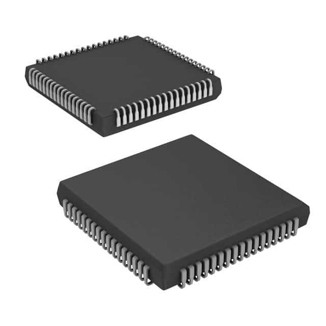
Package
The A40MX02-2PL68 comes in a compact package that ensures easy integration into electronic systems. The package type is PLCC (Plastic Leaded Chip Carrier).
Essence
The essence of this product lies in its ability to provide reconfigurable logic functionality, allowing designers to implement custom logic circuits without the need for dedicated hardware.
Packaging/Quantity
The A40MX02-2PL68 is typically packaged in reels or tubes, depending on the manufacturer's specifications. The quantity per package may vary but is commonly around 100 units.
Specifications
- Device Type: Programmable Logic Device (PLD)
- Family: A40MX
- Model: A40MX02-2PL68
- Logic Elements: 2,000
- I/O Pins: 68
- Operating Voltage: 3.3V
- Package Type: PLCC
- Package Dimensions: 20mm x 20mm
Detailed Pin Configuration
The A40MX02-2PL68 has a total of 68 I/O pins. These pins are used for input/output connections and configuration purposes. The pin configuration is as follows:
(Pin Number) - (Pin Name) 1 - IO0 2 - IO1 3 - IO2 ... 68 - IO67
Functional Features
- Reconfigurable Logic: The A40MX02-2PL68 allows users to modify the logic functions it performs, providing flexibility in circuit design.
- High-Speed Operation: The device offers fast switching speeds, enabling efficient data processing.
- I/O Flexibility: With 68 I/O pins, it provides ample connectivity options for interfacing with other components.
- Low Power Consumption: The A40MX02-2PL68 is designed to operate efficiently with minimal power consumption.
Advantages and Disadvantages
Advantages
- Flexibility in circuit design
- High-density logic elements
- Fast operation
- Ample I/O connectivity options
Disadvantages
- Limited availability of alternative models
- Programming complexity for inexperienced users
Working Principles
The A40MX02-2PL68 operates based on the principles of programmable logic. It consists of configurable logic blocks (CLBs), interconnect resources, and input/output blocks (IOBs). The CLBs can be programmed to implement various logic functions, while the interconnect resources allow for the routing of signals between different blocks. The IOBs provide the interface between the device and external components.
Detailed Application Field Plans
The A40MX02-2PL68 finds applications in various fields, including: - Digital signal processing - Communication systems - Industrial automation - Consumer electronics - Automotive electronics
In digital signal processing, it can be used for implementing filters, mathematical operations, and signal generation. In communication systems, it can be utilized for protocol handling, encryption/decryption, and error correction. In industrial automation, it can enable control and monitoring functions. In consumer electronics and automotive electronics, it can support various functionalities such as display control, sensor interfacing, and data processing.
Detailed and Complete Alternative Models
While the A40MX02-2PL68 is a reliable and versatile programmable logic device, there are alternative models available in the market that offer similar functionality. Some notable alternatives include:
- A40MX04-2PL68: This model offers double the number of logic elements compared to the A40MX02-2PL68, providing increased design capacity.
- A40MX01-3PL84: With a higher pin count, this model allows for more extensive I/O connectivity options.
- A40MX03-1PQ100: This alternative provides a different package type (PQFP) and a larger number of I/O pins, making it suitable for specific design requirements.
These alternative models can be considered based on specific project needs and compatibility requirements.
In conclusion, the A40MX02-2PL68 is a programmable logic device that offers flexibility, high-density logic elements, and low power consumption. Its reconfigurable nature makes it suitable for various applications in digital circuit design. While it has advantages such as fast operation and
10个与A40MX02-2PL68在技术解决方案中的应用相关的常见问题及解答
Sure! Here are 10 common questions and answers related to the application of A40MX02-2PL68 in technical solutions:
Q: What is A40MX02-2PL68? A: A40MX02-2PL68 is a specific model of field-programmable gate array (FPGA) manufactured by Microsemi Corporation.
Q: What are the key features of A40MX02-2PL68? A: Some key features of A40MX02-2PL68 include 2,000 usable gates, 68-pin PLCC package, 5V operation, and high-speed performance.
Q: How can A40MX02-2PL68 be used in technical solutions? A: A40MX02-2PL68 can be used in various technical solutions such as digital signal processing, data acquisition systems, industrial control systems, and communication equipment.
Q: What programming languages are supported by A40MX02-2PL68? A: A40MX02-2PL68 supports popular hardware description languages (HDLs) like VHDL and Verilog for programming and configuration.
Q: Can A40MX02-2PL68 be reprogrammed after deployment? A: Yes, A40MX02-2PL68 is a reprogrammable FPGA, allowing for flexibility and updates to the design even after deployment.
Q: What tools are available for programming A40MX02-2PL68? A: Microsemi provides software tools like Libero SoC Design Suite and Designer for programming and configuring A40MX02-2PL68.
Q: What is the power consumption of A40MX02-2PL68? A: The power consumption of A40MX02-2PL68 depends on the specific design and usage, but it is generally low compared to other FPGA models.
Q: Can A40MX02-2PL68 interface with external devices? A: Yes, A40MX02-2PL68 supports various communication interfaces like SPI, I2C, UART, and GPIOs, allowing it to interface with external devices.
Q: Are there any limitations or constraints when using A40MX02-2PL68? A: Some limitations include limited gate count, package size, and voltage compatibility (5V operation only). It's important to consider these factors during design.
Q: Where can I find more information about A40MX02-2PL68? A: You can find more detailed information about A40MX02-2PL68 in the datasheet provided by Microsemi Corporation or by visiting their official website.