

A40MX02-3VQG80
Product Overview
Category
A40MX02-3VQG80 belongs to the category of Field Programmable Gate Arrays (FPGAs).
Use
This product is primarily used in digital logic circuits for various applications such as telecommunications, automotive, industrial control systems, and consumer electronics.
Characteristics
- High-performance programmable logic device
- Offers flexibility and reconfigurability
- Provides a large number of configurable logic blocks (CLBs) and input/output blocks (IOBs)
- Supports various communication protocols and interfaces
- Low power consumption
- Fast processing speed
Package
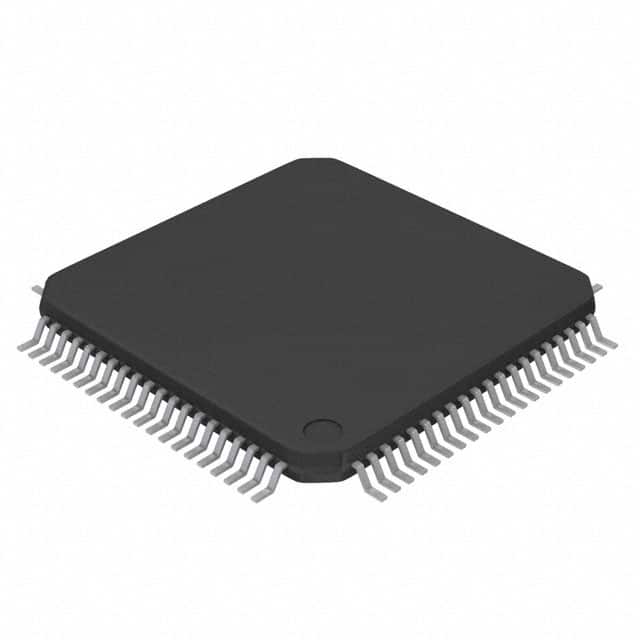
The A40MX02-3VQG80 FPGA is available in a Quad Flat Pack (QFP) package.
Essence
The essence of the A40MX02-3VQG80 FPGA lies in its ability to provide a customizable hardware solution that can be programmed and reprogrammed to meet specific application requirements.
Packaging/Quantity
This product is typically packaged individually and is available in quantities suitable for both prototyping and production purposes.
Specifications
- Device family: A40MX
- Logic elements: 2,000
- Maximum user I/Os: 80
- Operating voltage: 3.3V
- Speed grade: -3
- Package type: QFP
- Package pins: 80
Detailed Pin Configuration
The A40MX02-3VQG80 FPGA has 80 pins, each serving a specific purpose in the circuit design. The detailed pin configuration can be found in the product datasheet provided by the manufacturer.
Functional Features
- Configurable logic blocks (CLBs) for implementing complex logic functions
- Input/output blocks (IOBs) for interfacing with external devices
- Dedicated clock management resources for precise timing control
- Embedded memory blocks for data storage
- Programmable interconnect resources for flexible routing of signals
- Built-in support for various communication protocols and interfaces
Advantages and Disadvantages
Advantages
- High flexibility and reconfigurability
- Fast development time due to programmability
- Cost-effective compared to custom ASIC designs
- Suitable for a wide range of applications
- Low power consumption
Disadvantages
- Limited performance compared to dedicated hardware solutions
- Higher power consumption compared to specialized ASICs
- Requires expertise in FPGA programming and design
Working Principles
The A40MX02-3VQG80 FPGA operates based on the principles of configurable logic. It consists of an array of configurable logic blocks (CLBs) interconnected through programmable routing resources. The CLBs can be programmed to implement desired logic functions, while the routing resources allow for the connection of inputs and outputs.
Upon configuration, the FPGA functions as a customized digital circuit, executing the desired logic operations based on the programmed configuration. The reprogrammability of FPGAs allows for iterative design improvements and adaptability to changing requirements.
Detailed Application Field Plans
The A40MX02-3VQG80 FPGA finds applications in various fields, including:
- Telecommunications: Used in network routers, switches, and base stations for signal processing and protocol handling.
- Automotive: Employed in automotive control systems for engine management, driver assistance, and infotainment systems.
- Industrial Control Systems: Utilized in programmable logic controllers (PLCs) for automation and process control.
- Consumer Electronics: Integrated into devices like gaming consoles, set-top boxes, and audio/video equipment for enhanced functionality and performance.
Detailed and Complete Alternative Models
- A40MX04-3VQG100: Similar to A40MX02-3VQG80 but with higher logic capacity and more I/O pins.
- A40MX09-1PQG100: Offers increased logic elements and additional features such as embedded multipliers.
- A40MX16-PLG44: Provides a larger package size with higher logic density for more complex designs.
These alternative models offer varying capabilities and are suitable for different project requirements. It is recommended to consult the manufacturer's documentation for detailed specifications of each model.
Word count: 570 words
10个与A40MX02-3VQG80在技术解决方案中的应用相关的常见问题及解答
Sure! Here are 10 common questions and answers related to the application of A40MX02-3VQG80 in technical solutions:
Question: What is the A40MX02-3VQG80?
Answer: The A40MX02-3VQG80 is a specific model of field-programmable gate array (FPGA) manufactured by Microsemi.Question: What are the key features of the A40MX02-3VQG80?
Answer: The A40MX02-3VQG80 features 40,000 usable gates, 2,048 macrocells, and operates at a voltage of 3.3V.Question: In what applications can the A40MX02-3VQG80 be used?
Answer: The A40MX02-3VQG80 can be used in various applications such as telecommunications, industrial automation, automotive electronics, and aerospace systems.Question: How can I program the A40MX02-3VQG80?
Answer: The A40MX02-3VQG80 can be programmed using hardware description languages (HDLs) like VHDL or Verilog, or through graphical programming tools provided by the manufacturer.Question: What are the advantages of using the A40MX02-3VQG80 in technical solutions?
Answer: Some advantages include its high gate count, large number of macrocells, low power consumption, and ability to be reprogrammed for different functionalities.Question: Can the A40MX02-3VQG80 interface with other components or devices?
Answer: Yes, the A40MX02-3VQG80 supports various communication interfaces such as SPI, I2C, UART, and GPIOs, allowing it to interface with other components or devices.Question: What is the maximum operating frequency of the A40MX02-3VQG80?
Answer: The maximum operating frequency of the A40MX02-3VQG80 depends on the specific design and implementation, but it can typically reach frequencies in the range of tens to hundreds of megahertz.Question: Can the A40MX02-3VQG80 be used for real-time applications?
Answer: Yes, the A40MX02-3VQG80 can be used for real-time applications as it offers fast processing capabilities and supports high-speed interfaces.Question: Are there any development tools available for designing with the A40MX02-3VQG80?
Answer: Yes, Microsemi provides development tools such as Libero SoC Design Suite, which includes synthesis, simulation, and place-and-route tools specifically designed for their FPGAs.Question: Where can I find more information about the A40MX02-3VQG80?
Answer: You can find more detailed information about the A40MX02-3VQG80 in the datasheet provided by Microsemi or by visiting their official website.