

A40MX02-FPQG100
Product Overview
Category
The A40MX02-FPQG100 belongs to the category of Field-Programmable Gate Arrays (FPGAs).
Use
This FPGA is commonly used in electronic circuits for various applications, including digital signal processing, telecommunications, and embedded systems.
Characteristics
- High-performance programmable logic device
- Offers flexibility and reconfigurability
- Provides a large number of configurable logic blocks and input/output pins
- Supports complex digital designs
Package
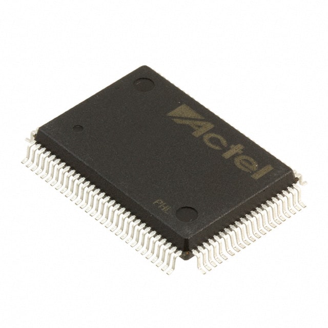
The A40MX02-FPQG100 comes in a compact quad flat package (QFP) form factor.
Essence
The essence of this FPGA lies in its ability to be programmed and reprogrammed to perform specific functions, making it highly versatile and adaptable to different design requirements.
Packaging/Quantity
Each package contains one A40MX02-FPQG100 FPGA.
Specifications
- Logic elements: 2,000
- Maximum user I/Os: 100
- Operating voltage: 3.3V
- Speed grade: Fast propagation delay
Detailed Pin Configuration
The A40MX02-FPQG100 has a total of 100 pins, which are assigned for various purposes such as input, output, power supply, and configuration. The detailed pin configuration can be found in the product datasheet.
Functional Features
- High-speed Performance: The A40MX02-FPQG100 offers fast propagation delay, enabling efficient execution of complex digital designs.
- Reconfigurability: This FPGA allows users to modify the circuitry and functionality even after deployment, providing flexibility for future design changes.
- Large Logic Capacity: With 2,000 logic elements, the A40MX02-FPQG100 can accommodate intricate digital designs.
- Versatile I/O Options: The FPGA provides 100 user I/Os, allowing for seamless integration with external devices and peripherals.
Advantages and Disadvantages
Advantages
- Flexibility in design modifications
- High-performance capabilities
- Large logic capacity
- Versatile I/O options
Disadvantages
- Steeper learning curve compared to fixed-function integrated circuits
- Higher power consumption compared to dedicated hardware solutions
Working Principles
The A40MX02-FPQG100 operates based on the principles of reconfigurable computing. It consists of configurable logic blocks (CLBs), interconnect resources, and input/output blocks (IOBs). The CLBs can be programmed to implement various digital functions, while the interconnect resources facilitate communication between different components within the FPGA. The IOBs provide interfaces for connecting external devices.
Detailed Application Field Plans
The A40MX02-FPQG100 finds applications in a wide range of fields, including: 1. Digital signal processing: Used for real-time audio and video processing. 2. Telecommunications: Employed in network routers, switches, and base stations. 3. Embedded systems: Integrated into automotive electronics, industrial control systems, and consumer electronics.
Detailed and Complete Alternative Models
- A40MX04-FPQG144: Similar to A40MX02-FPQG100 but offers higher logic capacity with 4,000 logic elements.
- A40MX09-FPQG208: Provides even larger logic capacity with 9,000 logic elements, suitable for more complex designs.
- A40MX16-FPQG240: Offers the highest logic capacity among the series, featuring 16,000 logic elements for demanding applications.
These alternative models provide increased logic capacity, catering to diverse design requirements.
Word count: 530 words
10个与A40MX02-FPQG100在技术解决方案中的应用相关的常见问题及解答
Sure! Here are 10 common questions and answers related to the application of A40MX02-FPQG100 in technical solutions:
Question: What is the A40MX02-FPQG100?
Answer: The A40MX02-FPQG100 is a field-programmable gate array (FPGA) manufactured by Microsemi Corporation.Question: What are the key features of the A40MX02-FPQG100?
Answer: Some key features of the A40MX02-FPQG100 include 40,000 usable gates, 2,048 macrocells, and 100-pin quad flat pack (QFP) package.Question: What is the typical power consumption of the A40MX02-FPQG100?
Answer: The typical power consumption of the A40MX02-FPQG100 is around 200 milliwatts.Question: Can the A40MX02-FPQG100 be used for digital signal processing (DSP) applications?
Answer: Yes, the A40MX02-FPQG100 can be used for DSP applications as it supports various arithmetic functions and has dedicated resources for implementing DSP algorithms.Question: What programming languages can be used to program the A40MX02-FPQG100?
Answer: The A40MX02-FPQG100 can be programmed using hardware description languages (HDLs) such as VHDL or Verilog.Question: Is the A40MX02-FPQG100 suitable for high-speed communication protocols?
Answer: Yes, the A40MX02-FPQG100 supports various high-speed communication protocols like Ethernet, PCI, and USB.Question: Can the A40MX02-FPQG100 be used in safety-critical applications?
Answer: Yes, the A40MX02-FPQG100 can be used in safety-critical applications as it supports built-in error detection and correction mechanisms.Question: What is the maximum operating frequency of the A40MX02-FPQG100?
Answer: The maximum operating frequency of the A40MX02-FPQG100 is typically around 200 MHz.Question: Can the A40MX02-FPQG100 be reprogrammed multiple times?
Answer: Yes, the A40MX02-FPQG100 is a reprogrammable FPGA, allowing for multiple programming cycles.Question: Are there any development tools available for programming the A40MX02-FPQG100?
Answer: Yes, Microsemi provides development tools like Libero SoC Design Suite that can be used to program and configure the A40MX02-FPQG100.
Please note that the answers provided here are general and may vary based on specific application requirements and manufacturer specifications.