

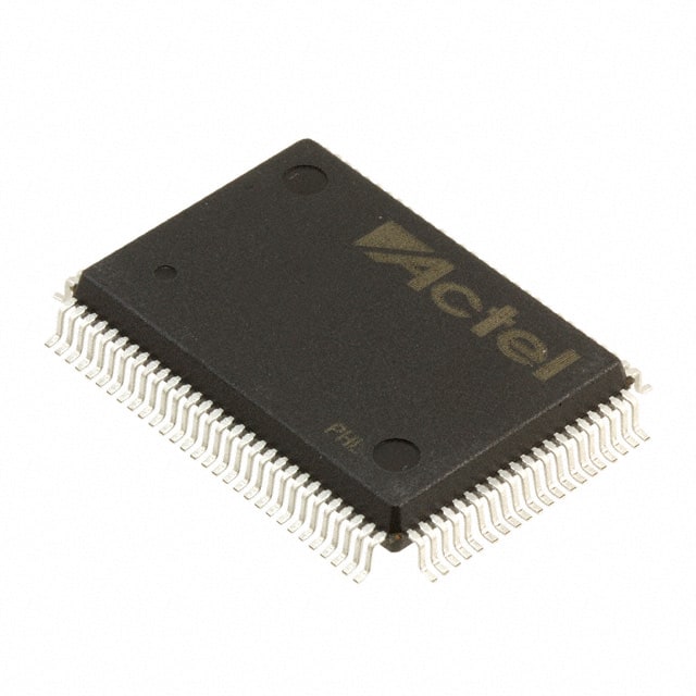
A40MX02-PQ100A
Product Overview
Category
The A40MX02-PQ100A belongs to the category of programmable logic devices (PLDs).
Use
This device is primarily used for digital circuit design and implementation. It provides a flexible and customizable solution for various applications.
Characteristics
- Programmable: The A40MX02-PQ100A can be programmed to perform specific functions, allowing for versatile use.
- High Integration: This PLD offers a high level of integration, enabling complex designs to be implemented on a single chip.
- Low Power Consumption: The device is designed to operate efficiently with low power consumption.
- Fast Operation: With its advanced architecture, the A40MX02-PQ100A delivers fast operation speeds.
Package
The A40MX02-PQ100A is available in a PQ100 package, which refers to a plastic quad flat pack with 100 pins.
Essence
The essence of the A40MX02-PQ100A lies in its ability to provide reconfigurable logic functions, allowing designers to create custom digital circuits without the need for dedicated hardware.
Packaging/Quantity
The A40MX02-PQ100A is typically packaged individually and is available in various quantities depending on the supplier.
Specifications
- Logic Cells: 2,000
- Maximum Frequency: 100 MHz
- I/O Pins: 100
- Operating Voltage: 3.3V
- Operating Temperature: -40°C to 85°C
- Programming Technology: In-System Programmable (ISP)
Detailed Pin Configuration
The A40MX02-PQ100A has a total of 100 pins, each serving a specific purpose in the device's functionality. The pin configuration is as follows:
(Pin Number) (Pin Name) (Description) 1 VCC Power Supply 2 GND Ground 3 IO1 Input/Output Pin 1 4 IO2 Input/Output Pin 2 ... 100 IO100 Input/Output Pin 100
Functional Features
- Reconfigurable Logic: The A40MX02-PQ100A allows users to modify the logic functions of the device, providing flexibility in circuit design.
- Embedded Memory: This PLD includes embedded memory blocks, enabling storage and retrieval of data within the device itself.
- Clock Management: The device offers built-in clock management features, allowing precise control over timing requirements.
- I/O Flexibility: With 100 I/O pins, the A40MX02-PQ100A provides ample connectivity options for interfacing with external devices.
Advantages and Disadvantages
Advantages
- Versatility: The reprogrammable nature of the A40MX02-PQ100A makes it suitable for a wide range of applications.
- Cost-Effective: By eliminating the need for dedicated hardware, this PLD reduces overall system costs.
- Time-Saving: Design iterations can be quickly implemented by reprogramming the device, saving valuable development time.
Disadvantages
- Limited Resources: Compared to larger PLDs or FPGAs, the A40MX02-PQ100A has a limited number of logic cells and I/O pins.
- Complexity: Programming and configuring the device may require specialized knowledge and tools.
Working Principles
The A40MX02-PQ100A utilizes a matrix of configurable logic elements interconnected through programmable routing resources. These elements can be programmed to implement various logic functions, allowing designers to create custom digital circuits. The device operates based on the user-defined configuration, executing the desired functionality.
Detailed Application Field Plans
The A40MX02-PQ100A finds applications in various fields, including:
- Communications: Used in networking equipment, routers, and switches for data processing and protocol handling.
- Industrial Automation: Employed in control systems, PLCs, and robotics for real-time control and signal processing.
- Consumer Electronics: Integrated into smart devices, gaming consoles, and multimedia systems for custom functionality.
- Automotive: Utilized in automotive electronics for engine control, driver assistance systems, and infotainment.
Detailed and Complete Alternative Models
- A40MX04-PQ100A: Similar to the A40MX02-PQ100A but with double the logic cells and I/O pins.
- A40MX08-PQ100A: Offers four times the logic cells and I/O pins compared to the A40MX02-PQ100A.
- A40MX16-PQ100A: Provides eight times the logic cells and I/O pins compared to the A40MX02-PQ100A.
These alternative models offer increased resources for more complex designs but may come at a higher cost.
Word count: 609 words
10个与A40MX02-PQ100A在技术解决方案中的应用相关的常见问题及解答
Sure! Here are 10 common questions and answers related to the application of A40MX02-PQ100A in technical solutions:
Question: What is the A40MX02-PQ100A?
Answer: The A40MX02-PQ100A is a specific model of field-programmable gate array (FPGA) manufactured by Microsemi Corporation.Question: What are the key features of the A40MX02-PQ100A?
Answer: Some key features of the A40MX02-PQ100A include 40,000 usable gates, 2,048 macrocells, 64 I/O pins, and a PQ100 package.Question: In what types of technical solutions can the A40MX02-PQ100A be used?
Answer: The A40MX02-PQ100A can be used in various applications such as telecommunications, industrial automation, automotive electronics, and more.Question: How does the A40MX02-PQ100A differ from other FPGAs?
Answer: The A40MX02-PQ100A offers a balance between cost, performance, and power consumption, making it suitable for many general-purpose applications.Question: Can the A40MX02-PQ100A be reprogrammed after deployment?
Answer: Yes, the A40MX02-PQ100A is a field-programmable device, meaning it can be reprogrammed even after it has been deployed in a system.Question: What development tools are available for programming the A40MX02-PQ100A?
Answer: Microsemi provides a range of development tools, including software like Libero SoC Design Suite and SmartFusion2 Creative Development Kit, which can be used to program the A40MX02-PQ100A.Question: What is the power supply requirement for the A40MX02-PQ100A?
Answer: The A40MX02-PQ100A typically operates on a 3.3V power supply, but it also supports a wide voltage range from 2.375V to 3.465V.Question: Can the A40MX02-PQ100A interface with other components or devices?
Answer: Yes, the A40MX02-PQ100A has multiple I/O pins that can be used to interface with other components or devices in a system.Question: Are there any limitations or considerations when using the A40MX02-PQ100A?
Answer: Some considerations include the available resources (gates, macrocells) and the specific requirements of your application. It's important to consult the datasheet and design guidelines provided by Microsemi.Question: Where can I find additional technical documentation and support for the A40MX02-PQ100A?
Answer: You can find additional technical documentation, datasheets, application notes, and support resources on the Microsemi Corporation website or by contacting their customer support team.