

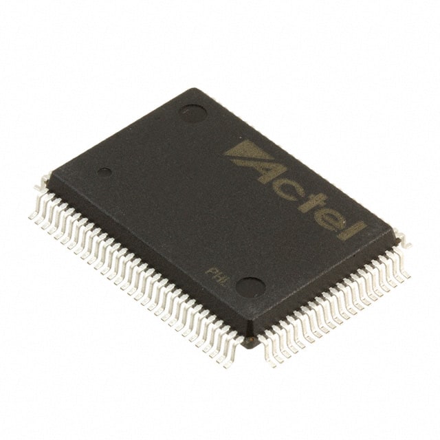
A40MX02-PQG100A
Product Overview
Category
The A40MX02-PQG100A belongs to the category of programmable logic devices (PLDs).
Use
This device is primarily used for digital circuit design and implementation. It offers a flexible and customizable solution for various applications.
Characteristics
- Programmable: The A40MX02-PQG100A can be programmed to perform specific functions based on user requirements.
- High Integration: This device integrates multiple logic gates, flip-flops, and other components into a single chip.
- Versatile: It supports a wide range of applications due to its programmability.
- Low Power Consumption: The A40MX02-PQG100A is designed to operate efficiently with minimal power consumption.
Package
The A40MX02-PQG100A is available in a PQG100A package.
Essence
The essence of the A40MX02-PQG100A lies in its ability to provide a reconfigurable hardware platform that allows users to implement complex digital circuits.
Packaging/Quantity
This product is typically packaged individually and is available in various quantities depending on customer requirements.
Specifications
- Logic Cells: 2,000
- Maximum Frequency: 100 MHz
- I/O Pins: 100
- Operating Voltage: 3.3V
- Package Type: PQG100A
- Temperature Range: -40°C to +85°C
Detailed Pin Configuration
The A40MX02-PQG100A has a total of 100 pins. The pin configuration is as follows:
(Pin Number) (Pin Name) 1. VCCIO 2. GND 3. IO0 4. IO1 5. IO2 6. IO3 7. IO4 8. IO5 9. IO6 10. IO7 11. ... ... 100. GND
Functional Features
- Reconfigurable Logic: The A40MX02-PQG100A allows users to modify the logic functions and interconnections within the device, providing flexibility in circuit design.
- Fast Turnaround Time: With its programmable nature, this device enables rapid prototyping and iterative design cycles.
- High-Speed Performance: The A40MX02-PQG100A operates at a maximum frequency of 100 MHz, making it suitable for applications requiring high-speed data processing.
- I/O Flexibility: It offers a generous number of I/O pins (100) to accommodate various input and output requirements.
Advantages and Disadvantages
Advantages
- Versatility: The A40MX02-PQG100A can be used in a wide range of applications due to its programmability.
- Cost-Effective: By eliminating the need for custom-designed circuits, this device reduces development costs.
- Time-Saving: Its reprogrammable nature allows for quick modifications and updates without requiring hardware changes.
Disadvantages
- Limited Complexity: While the A40MX02-PQG100A is capable of implementing complex digital circuits, it may have limitations compared to more advanced PLDs or FPGAs.
- Learning Curve: Utilizing the full potential of this device requires knowledge of hardware description languages and digital circuit design principles.
Working Principles
The A40MX02-PQG100A utilizes a combination of configurable logic blocks, interconnect resources, and I/O elements to implement user-defined digital circuits. These circuits are programmed using hardware description languages (HDLs) such as VHDL or Verilog. Upon programming, the device configures its internal components to realize the desired functionality.
Detailed Application Field Plans
The A40MX02-PQG100A finds applications in various fields, including: - Industrial Automation - Communications Systems - Consumer Electronics - Automotive Electronics - Medical Devices
Detailed and Complete Alternative Models
- A40MX04-PQG100A: Similar to the A40MX02-PQG100A but with double the logic cells (4,000).
- A40MX08-PQG100A: Offers eight times the logic cells (8,000) compared to the A40MX02-PQG100A.
- A40MX16-PQG100A: Provides sixteen times the logic cells (16,000) for more complex circuit designs.
These alternative models offer increased capacity and capabilities for users requiring higher logic density.
Word count: 607 words
10个与A40MX02-PQG100A在技术解决方案中的应用相关的常见问题及解答
Sure! Here are 10 common questions and answers related to the application of A40MX02-PQG100A in technical solutions:
Question: What is the A40MX02-PQG100A?
Answer: The A40MX02-PQG100A is a specific model of field-programmable gate array (FPGA) manufactured by Microsemi Corporation.Question: What are the key features of the A40MX02-PQG100A?
Answer: Some key features of the A40MX02-PQG100A include 40,000 usable gates, 2,048 macrocells, 64 I/O pins, and support for various I/O standards.Question: In what applications can the A40MX02-PQG100A be used?
Answer: The A40MX02-PQG100A can be used in a wide range of applications such as telecommunications, industrial automation, medical devices, aerospace, and more.Question: How can I program the A40MX02-PQG100A?
Answer: The A40MX02-PQG100A can be programmed using hardware description languages (HDLs) like VHDL or Verilog, and then synthesized and implemented using appropriate software tools.Question: Can the A40MX02-PQG100A be reprogrammed after deployment?
Answer: Yes, the A40MX02-PQG100A is a reprogrammable FPGA, allowing you to modify its functionality even after it has been deployed in a system.Question: What are the power requirements for the A40MX02-PQG100A?
Answer: The A40MX02-PQG100A typically operates at a voltage range of 3.3V, but it is important to refer to the datasheet for specific power requirements.Question: Does the A40MX02-PQG100A support external memory interfaces?
Answer: Yes, the A40MX02-PQG100A supports various external memory interfaces such as SRAM, SDRAM, and Flash memory.Question: Can I use the A40MX02-PQG100A in a high-speed data processing application?
Answer: Yes, the A40MX02-PQG100A offers features like high-speed I/O pins and dedicated clock management resources, making it suitable for high-speed data processing applications.Question: Are there any development boards or evaluation kits available for the A40MX02-PQG100A?
Answer: Yes, Microsemi provides development boards and evaluation kits specifically designed for the A40MX02-PQG100A, which can help in prototyping and testing.Question: Where can I find technical documentation and support for the A40MX02-PQG100A?
Answer: You can find technical documentation, datasheets, application notes, and support resources on the official Microsemi website or by contacting their customer support team.