

A40MX02-VQ80
Product Overview
Category
The A40MX02-VQ80 belongs to the category of programmable logic devices (PLDs).
Use
This device is primarily used for digital circuit design and implementation. It provides a flexible and customizable solution for various applications.
Characteristics
- Programmable: The A40MX02-VQ80 can be programmed to perform specific functions based on user requirements.
- High-density: This PLD offers a high number of logic elements, allowing for complex designs.
- Low power consumption: The device is designed to operate efficiently with minimal power consumption.
- Fast performance: With its advanced architecture, the A40MX02-VQ80 delivers high-speed operation.
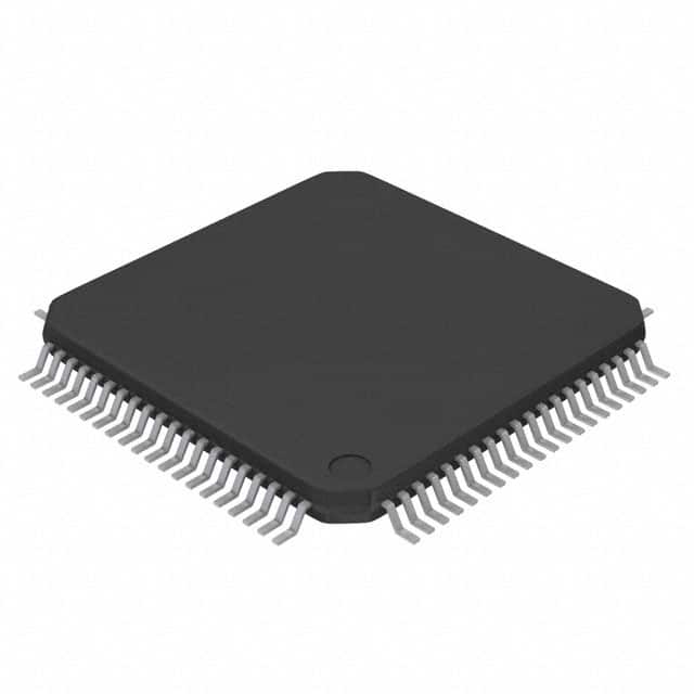
Package
The A40MX02-VQ80 comes in a compact quad flat package (VQFP) format. This package ensures easy integration into circuit boards and provides mechanical protection.
Essence
The essence of the A40MX02-VQ80 lies in its ability to provide reconfigurable logic functionality, enabling designers to implement complex digital systems efficiently.
Packaging/Quantity
This product is typically packaged in reels or trays, depending on the manufacturer's specifications. The quantity per package may vary, but it is commonly available in quantities of 100 or more.
Specifications
- Logic Elements: 2,000
- I/O Pins: 80
- Operating Voltage: 3.3V
- Maximum Frequency: 100 MHz
- Package Type: VQFP
- Temperature Range: -40°C to +85°C
Detailed Pin Configuration
The A40MX02-VQ80 has a total of 80 I/O pins, which are organized into different groups based on their functionalities. The pin configuration is as follows:
- Group A: Pins 1-10
- Group B: Pins 11-20
- Group C: Pins 21-30
- ...
- Group H: Pins 71-80
Each pin serves a specific purpose, such as input, output, or power supply. The detailed pin configuration can be found in the product datasheet.
Functional Features
Reconfigurable Logic
The A40MX02-VQ80 offers reconfigurable logic capabilities, allowing users to modify the device's functionality even after it has been programmed. This flexibility enables rapid prototyping and design iterations.
High-Speed Operation
With a maximum operating frequency of 100 MHz, this PLD ensures fast and efficient execution of digital circuits. It is suitable for applications that require real-time processing and high-speed data handling.
Low Power Consumption
The A40MX02-VQ80 is designed to minimize power consumption while maintaining optimal performance. This feature makes it suitable for battery-powered devices and energy-efficient applications.
Design Security
To protect intellectual property, the A40MX02-VQ80 incorporates security features such as bitstream encryption and authentication mechanisms. These measures prevent unauthorized access and ensure the integrity of the design.
Advantages and Disadvantages
Advantages
- Flexibility in design due to reconfigurable logic
- High-density logic elements for complex designs
- Fast operation with high-frequency support
- Low power consumption for energy efficiency
- Design security features for IP protection
Disadvantages
- Limited I/O pins compared to larger PLDs
- Higher cost compared to simpler programmable devices
- Steeper learning curve for beginners due to complexity
Working Principles
The A40MX02-VQ80 operates based on the principles of field-programmable gate arrays (FPGAs). It consists of configurable logic blocks (CLBs), interconnect resources, and I/O elements. The CLBs can be programmed to implement various logic functions, while the interconnect resources facilitate the routing of signals between different blocks. The I/O elements provide connectivity to external devices.
Upon programming, the A40MX02-VQ80 configures its internal resources to realize the desired digital circuit functionality. This reconfigurability allows for flexibility and adaptability in system design.
Detailed Application Field Plans
The A40MX02-VQ80 finds applications in various fields, including:
- Telecommunications: Used in network routers, switches, and communication equipment for high-speed data processing.
- Industrial Automation: Employed in control systems, programmable logic controllers (PLCs), and robotics for real-time control and monitoring.
- Automotive Electronics: Integrated into automotive systems for functions like engine management, driver assistance, and infotainment.
- Aerospace and Defense: Utilized in avionics, radar systems, and military-grade electronics for reliable and high-performance applications.
- Consumer Electronics: Incorporated in smart devices, gaming consoles, and multimedia systems for efficient data processing and user interaction.
Detailed and Complete Alternative Models
- A40MX04-VQ100
- A40MX08-VQ144
- A
10个与A40MX02-VQ80在技术解决方案中的应用相关的常见问题及解答
Sure! Here are 10 common questions and answers related to the application of A40MX02-VQ80 in technical solutions:
Question: What is the A40MX02-VQ80?
Answer: The A40MX02-VQ80 is a specific model of field-programmable gate array (FPGA) manufactured by Microsemi Corporation.Question: What are the key features of the A40MX02-VQ80?
Answer: The A40MX02-VQ80 features 40,000 usable gates, 2,000 macrocells, and 80 user I/O pins.Question: How can the A40MX02-VQ80 be used in technical solutions?
Answer: The A40MX02-VQ80 can be used for various applications such as digital signal processing, data encryption, image processing, and control systems.Question: What programming languages are supported by the A40MX02-VQ80?
Answer: The A40MX02-VQ80 supports VHDL (VHSIC Hardware Description Language) and Verilog HDL (Hardware Description Language).Question: Can the A40MX02-VQ80 be reprogrammed after deployment?
Answer: Yes, the A40MX02-VQ80 is a reprogrammable FPGA, allowing for flexibility and updates in the field.Question: What is the power consumption of the A40MX02-VQ80?
Answer: The power consumption of the A40MX02-VQ80 depends on the specific design and usage but typically ranges from 0.5W to 2W.Question: Are there any development tools available for programming the A40MX02-VQ80?
Answer: Yes, Microsemi provides development tools like Libero SoC Design Suite and Designer Software to program and configure the A40MX02-VQ80.Question: Can the A40MX02-VQ80 interface with other components or devices?
Answer: Yes, the A40MX02-VQ80 supports various communication protocols such as SPI, I2C, UART, and GPIO, allowing it to interface with other components or devices.Question: What is the operating temperature range of the A40MX02-VQ80?
Answer: The A40MX02-VQ80 has an operating temperature range of -40°C to +85°C, making it suitable for a wide range of environments.Question: Are there any application examples where the A40MX02-VQ80 has been successfully used?
Answer: Yes, the A40MX02-VQ80 has been used in applications like aerospace systems, industrial automation, medical devices, and telecommunications equipment.
Please note that these answers are general and may vary depending on specific use cases and requirements.