

A40MX04-1PLG68
Product Overview
Category
A40MX04-1PLG68 belongs to the category of programmable logic devices (PLDs).
Use
This product is primarily used in digital circuit design and implementation. It provides a flexible and customizable solution for various applications.
Characteristics
- Programmable: The A40MX04-1PLG68 can be programmed to perform specific functions based on user requirements.
- High Integration: It offers a high level of integration, allowing for complex designs to be implemented on a single chip.
- Versatile: The device supports a wide range of applications due to its programmability.
- Low Power Consumption: A40MX04-1PLG68 is designed to operate efficiently with low power consumption.
- Reliable: It ensures reliable performance and stability in different operating conditions.
Package
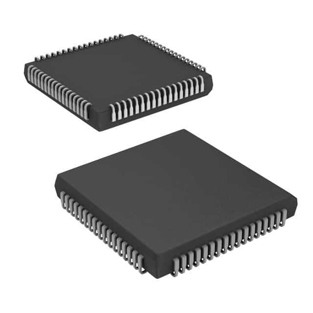
The A40MX04-1PLG68 comes in a PLCC-68 package.
Essence
The essence of this product lies in its ability to provide a reconfigurable hardware platform that allows users to implement custom digital circuits.
Packaging/Quantity
The A40MX04-1PLG68 is typically packaged individually and is available in various quantities depending on the manufacturer's specifications.
Specifications
- Logic Elements: 4000
- Macrocells: 128
- I/O Pins: 68
- Operating Voltage: 3.3V
- Speed Grade: Standard (5ns)
Detailed Pin Configuration
The A40MX04-1PLG68 has a total of 68 pins, each serving a specific purpose in the device's functionality. The pin configuration is as follows:
(Pin Number) - (Pin Name) - (Function) 1 - VCCIO - Power Supply for I/O Buffers 2 - GND - Ground 3 - TCK - Test Clock Input 4 - TMS - Test Mode Select 5 - TDI - Test Data Input 6 - TDO - Test Data Output 7 - VCC - Power Supply 8 - GND - Ground 9 - IO1 - I/O Pin 1 10 - IO2 - I/O Pin 2 ... 68 - IO68 - I/O Pin 68
Functional Features
- Reconfigurability: The A40MX04-1PLG68 can be reprogrammed multiple times, allowing for design changes and updates.
- In-system Programming: It supports in-system programming, enabling users to update the device without removing it from the circuit.
- JTAG Interface: The device features a JTAG interface for easy debugging and testing of the implemented design.
- High-Speed Operation: A40MX04-1PLG68 operates at high speeds, making it suitable for applications that require fast data processing.
Advantages and Disadvantages
Advantages
- Flexibility: The programmable nature of this device offers flexibility in designing various digital circuits.
- Cost-Effective: A single A40MX04-1PLG68 can replace multiple discrete components, reducing overall system costs.
- Time-Saving: The reconfigurable nature of the device allows for quick prototyping and design iterations.
- Integration: The high level of integration simplifies circuit board layout and reduces space requirements.
Disadvantages
- Complexity: Programming and configuring the device may require specialized knowledge and expertise.
- Limited Resources: The number of logic elements and macrocells may not be sufficient for highly complex designs.
- Power Consumption: While designed for low power consumption, certain configurations may result in higher power usage.
Working Principles
The A40MX04-1PLG68 utilizes a matrix of configurable logic blocks interconnected through programmable routing resources. These logic blocks can be programmed to perform specific functions and are interconnected to create the desired digital circuit. The device's configuration is stored in non-volatile memory, allowing it to retain the programmed design even when powered off.
Detailed Application Field Plans
The A40MX04-1PLG68 finds applications in various fields, including:
- Telecommunications: Used in network equipment for signal processing and protocol implementation.
- Industrial Automation: Employed in control systems for process monitoring and automation.
- Consumer Electronics: Integrated into devices like gaming consoles and multimedia players for custom functionality.
- Automotive: Utilized in automotive electronics for engine management, driver assistance systems, and infotainment.
- Medical Devices: Incorporated into medical equipment for data acquisition, signal processing, and control.
Detailed and Complete Alternative Models
- A40MX02-1PLG44: Similar to A40MX04-1PLG68 but with 2000 logic elements and 64 I/O pins.
- A40MX09-1PLG84: Offers increased capacity with 9000 logic elements and 84 I/O pins.
- A40MX16-1
10个与A40MX04-1PLG68在技术解决方案中的应用相关的常见问题及解答
Sure! Here are 10 common questions and answers related to the application of A40MX04-1PLG68 in technical solutions:
Q1: What is A40MX04-1PLG68? A1: A40MX04-1PLG68 is a specific model of field-programmable gate array (FPGA) manufactured by Microsemi Corporation.
Q2: What are the key features of A40MX04-1PLG68? A2: Some key features of A40MX04-1PLG68 include 4,000 logic cells, 68-pin PLCC package, 3.3V operation, and support for various I/O standards.
Q3: What is the typical application of A40MX04-1PLG68? A3: A40MX04-1PLG68 is commonly used in applications such as industrial control systems, telecommunications equipment, and automotive electronics.
Q4: How can I program A40MX04-1PLG68? A4: A40MX04-1PLG68 can be programmed using hardware description languages (HDLs) like VHDL or Verilog, and then configured using programming tools provided by Microsemi.
Q5: Can A40MX04-1PLG68 be reprogrammed after initial configuration? A5: Yes, A40MX04-1PLG68 is a reprogrammable FPGA, allowing you to modify its functionality even after it has been initially configured.
Q6: What are the power requirements for A40MX04-1PLG68? A6: A40MX04-1PLG68 operates at a voltage of 3.3V and requires a stable power supply with appropriate current capabilities.
Q7: Does A40MX04-1PLG68 support different I/O standards? A7: Yes, A40MX04-1PLG68 supports various I/O standards such as LVCMOS, LVTTL, LVDS, and HSTL, making it versatile for interfacing with different devices.
Q8: Can A40MX04-1PLG68 interface with external memory devices? A8: Yes, A40MX04-1PLG68 has dedicated pins and features to interface with external memory devices like SRAM or SDRAM.
Q9: What is the maximum operating frequency of A40MX04-1PLG68? A9: The maximum operating frequency of A40MX04-1PLG68 depends on the specific design and implementation, but it can typically reach several hundred megahertz.
Q10: Are there any development tools available for A40MX04-1PLG68? A10: Yes, Microsemi provides development tools like Libero SoC Design Suite, which includes synthesis, simulation, and programming tools specifically designed for their FPGAs.
Please note that these answers are general and may vary depending on the specific requirements and use cases.