

A40MX04-3PLG84I
Product Overview
Category
A40MX04-3PLG84I belongs to the category of Field Programmable Gate Arrays (FPGAs).
Use
This product is primarily used in digital logic circuits for various applications such as telecommunications, automotive, industrial control systems, and consumer electronics.
Characteristics
- High-performance programmable logic device
- Offers flexibility and reconfigurability
- Provides a cost-effective solution for complex digital designs
- Supports high-speed data processing
- Low power consumption
- Compact size
Package
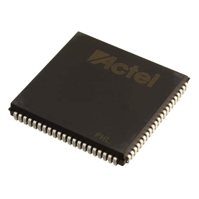
The A40MX04-3PLG84I comes in a PLCC-84 package.
Essence
The essence of this product lies in its ability to provide a customizable and versatile digital logic solution for a wide range of applications.
Packaging/Quantity
The A40MX04-3PLG84I is typically packaged individually and is available in various quantities depending on the manufacturer's specifications.
Specifications
- Logic Cells: 4,000
- Maximum Frequency: 200 MHz
- I/O Pins: 84
- Operating Voltage: 3.3V
- Operating Temperature Range: -40°C to +85°C
- Configuration Memory: Flash-based
Detailed Pin Configuration
The A40MX04-3PLG84I has 84 pins, each serving a specific purpose in the FPGA's functionality. The pin configuration includes input/output pins, clock pins, power supply pins, and configuration pins. For a detailed pin configuration diagram, please refer to the manufacturer's datasheet.
Functional Features
- Flexible and reprogrammable architecture
- Support for various communication protocols
- Built-in memory blocks for efficient data storage
- Dedicated arithmetic and logic units for mathematical operations
- On-chip PLLs for clock management
- Support for partial reconfiguration
Advantages and Disadvantages
Advantages
- Customizable to specific application requirements
- Faster time-to-market compared to custom ASIC designs
- Lower development costs
- Ability to make design changes even after deployment
- High-performance computing capabilities
Disadvantages
- Higher power consumption compared to dedicated hardware solutions
- Limited resources for complex designs
- Longer development time compared to off-the-shelf solutions
Working Principles
The A40MX04-3PLG84I is based on the principle of reconfigurable logic. It consists of a matrix of programmable logic cells interconnected through configurable routing resources. The device can be programmed using Hardware Description Languages (HDLs) such as VHDL or Verilog, which define the desired functionality of the digital circuit. Once programmed, the FPGA executes the logic operations according to the specified configuration.
Detailed Application Field Plans
The A40MX04-3PLG84I finds applications in various fields, including:
- Telecommunications: Used in base stations, network switches, and routers for signal processing and protocol handling.
- Automotive: Employed in automotive control systems for engine management, driver assistance, and infotainment systems.
- Industrial Control Systems: Utilized in industrial automation for process control, monitoring, and data acquisition.
- Consumer Electronics: Integrated into devices like gaming consoles, set-top boxes, and multimedia players for high-speed data processing and multimedia applications.
Detailed and Complete Alternative Models
- A40MX02-PLG68I: Similar to A40MX04-3PLG84I but with 2,000 logic cells and 68 I/O pins.
- A40MX09-FPLG115I: Offers increased capacity with 9,000 logic cells and 115 I/O pins.
- A40MX16-PQG100: Provides higher performance with 16,000 logic cells and a different package option.
These alternative models offer varying capabilities and pin configurations to suit different project requirements.
In conclusion, the A40MX04-3PLG84I is a versatile FPGA that provides a customizable and cost-effective solution for digital logic designs. Its high-performance computing capabilities, flexibility, and reconfigurability make it suitable for a wide range of applications in telecommunications, automotive, industrial control systems, and consumer electronics.
10个与A40MX04-3PLG84I在技术解决方案中的应用相关的常见问题及解答
What is the maximum operating frequency of A40MX04-3PLG84I?
- The maximum operating frequency of A40MX04-3PLG84I is 100 MHz.What are the typical applications for A40MX04-3PLG84I?
- A40MX04-3PLG84I is commonly used in industrial control, automotive, and consumer electronics applications.What is the power supply voltage range for A40MX04-3PLG84I?
- The power supply voltage range for A40MX04-3PLG84I is 3.0V to 3.6V.Can A40MX04-3PLG84I be reprogrammed after initial configuration?
- No, A40MX04-3PLG84I is a one-time programmable device and cannot be reprogrammed after initial configuration.What are the available I/O standards for A40MX04-3PLG84I?
- A40MX04-3PLG84I supports LVTTL, LVCMOS, and PCI I/O standards.Is A40MX04-3PLG84I suitable for high-reliability applications?
- Yes, A40MX04-3PLG84I is suitable for high-reliability applications due to its robust design and manufacturing process.What are the security features of A40MX04-3PLG84I?
- A40MX04-3PLG84I offers security features such as bitstream encryption and tamper detection.Can A40MX04-3PLG84I interface with external memory devices?
- Yes, A40MX04-3PLG84I can interface with external SRAM, Flash, and EEPROM devices.What development tools are available for A40MX04-3PLG84I?
- Development tools such as design software, programming hardware, and evaluation boards are available for A40MX04-3PLG84I.What are the temperature range specifications for A40MX04-3PLG84I?
- A40MX04-3PLG84I is specified to operate within a temperature range of -40°C to 85°C.