

A40MX04-3PQG100
Product Overview
Category
A40MX04-3PQG100 belongs to the category of Field Programmable Gate Arrays (FPGAs).
Use
This product is primarily used in digital logic circuits for various applications such as telecommunications, automotive, industrial control systems, and consumer electronics.
Characteristics
- High-performance FPGA with advanced programmable logic capabilities.
- Offers a wide range of configurable logic blocks and input/output resources.
- Provides flexibility in designing complex digital circuits.
- Supports reprogramming, allowing for iterative design improvements.
- Low power consumption compared to traditional ASICs (Application-Specific Integrated Circuits).
Package
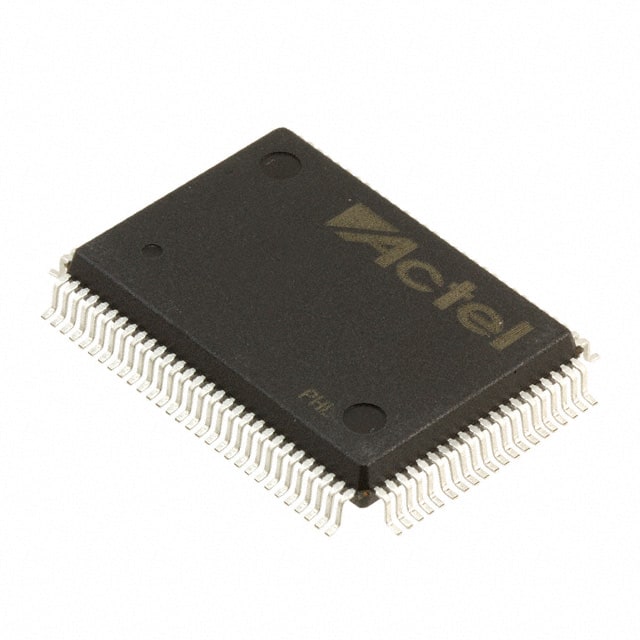
The A40MX04-3PQG100 comes in a compact Quad Flat Package (QFP) with 100 pins.
Essence
The essence of the A40MX04-3PQG100 lies in its ability to provide a customizable and reprogrammable digital logic solution for various applications.
Packaging/Quantity
This product is typically packaged in reels or trays, with each reel containing a specific quantity of A40MX04-3PQG100 FPGAs. The exact quantity may vary depending on the manufacturer's specifications.
Specifications
- Logic Elements: 4,000
- Maximum User I/Os: 96
- Embedded Multiplier Blocks: 20
- Block RAM: 144 Kbits
- Clock Management Tiles: 2
- Operating Voltage: 3.3V
- Speed Grade: -3
Detailed Pin Configuration
The A40MX04-3PQG100 has a total of 100 pins, each serving a specific purpose in the circuit design. The pin configuration includes input/output pins, power supply pins, ground pins, and configuration pins. For a detailed pin configuration diagram, please refer to the datasheet provided by the manufacturer.
Functional Features
- High-speed data processing capabilities.
- Configurable logic blocks for implementing complex digital functions.
- Flexible input/output resources for interfacing with external devices.
- On-chip memory blocks for efficient data storage and retrieval.
- Clock management tiles for precise timing control.
- Support for various communication protocols and interfaces.
Advantages and Disadvantages
Advantages
- Flexibility in design due to reprogrammability.
- Faster time-to-market compared to ASICs.
- Lower power consumption.
- Cost-effective for low to medium volume production.
- Ability to implement complex digital functions.
Disadvantages
- Limited performance compared to dedicated ASICs.
- Higher cost per unit compared to mass-produced ASICs.
- Limited scalability beyond a certain complexity level.
- Requires specialized knowledge for effective utilization.
Working Principles
The A40MX04-3PQG100 FPGA operates based on the principles of configurable logic. It consists of programmable logic blocks, interconnect resources, and input/output elements. The programmable logic blocks can be configured to implement desired digital functions using a Hardware Description Language (HDL) or a graphical design tool. The interconnect resources allow for the routing of signals between different logic blocks, enabling the creation of complex circuits. The input/output elements provide interfaces for connecting the FPGA to external devices.
Detailed Application Field Plans
The A40MX04-3PQG100 FPGA finds applications in various fields, including:
- Telecommunications: Used in base stations, network switches, and routers for signal processing, protocol conversion, and traffic management.
- Automotive: Employed in automotive control systems for engine management, driver assistance, and infotainment systems.
- Industrial Control Systems: Utilized in programmable logic controllers (PLCs), motor control systems, and factory automation equipment.
- Consumer Electronics: Integrated into high-definition televisions, gaming consoles, and audio/video processing devices for enhanced functionality.
Detailed and Complete Alternative Models
- A40MX02-3PQG100: Similar to A40MX04-3PQG100 but with a lower number of logic elements.
- A40MX08-3PQG100: Similar to A40MX04-3PQG100 but with a higher number of logic elements.
- A40MX16-3PQG100: Similar to A40MX04-3PQG100 but with an even higher number of logic elements.
These alternative models provide varying levels of logic resources to cater to different design requirements.
In conclusion, the A40MX04-3PQG100 FPGA is a versatile and flexible digital logic solution that finds applications in various industries. Its reprogrammability, configurable logic blocks, and extensive I/O resources make it suitable for implementing complex digital functions. While it has certain limitations compared to ASICs, its advantages in terms of flexibility, time-to-market, and power consumption make it a popular choice for many designers.
10个与A40MX04-3PQG100在技术解决方案中的应用相关的常见问题及解答
Sure! Here are 10 common questions and answers related to the application of A40MX04-3PQG100 in technical solutions:
Question: What is the A40MX04-3PQG100?
Answer: The A40MX04-3PQG100 is a specific model of field-programmable gate array (FPGA) manufactured by Microsemi.Question: What are the key features of the A40MX04-3PQG100?
Answer: The A40MX04-3PQG100 features 4,000 logic cells, 128 I/O pins, and operates at a maximum frequency of 100 MHz.Question: What are some typical applications for the A40MX04-3PQG100?
Answer: The A40MX04-3PQG100 is commonly used in various technical solutions such as industrial automation, telecommunications, aerospace, and defense systems.Question: How can I program the A40MX04-3PQG100?
Answer: The A40MX04-3PQG100 can be programmed using hardware description languages (HDLs) like VHDL or Verilog, and then configured using programming tools provided by Microsemi.Question: Can the A40MX04-3PQG100 be reprogrammed after initial configuration?
Answer: Yes, the A40MX04-3PQG100 is a reprogrammable FPGA, allowing for flexibility in design changes or updates.Question: What is the power supply requirement for the A40MX04-3PQG100?
Answer: The A40MX04-3PQG100 requires a single 3.3V power supply for operation.Question: Does the A40MX04-3PQG100 support external memory interfaces?
Answer: Yes, the A40MX04-3PQG100 supports various memory interfaces such as SRAM, SDRAM, and Flash memory.Question: Can I use the A40MX04-3PQG100 in a high-reliability application?
Answer: Yes, the A40MX04-3PQG100 is designed to meet stringent quality and reliability standards, making it suitable for high-reliability applications.Question: Are there any development boards or evaluation kits available for the A40MX04-3PQG100?
Answer: Yes, Microsemi offers development boards and evaluation kits specifically designed for the A40MX04-3PQG100, providing a convenient platform for prototyping and testing.Question: Where can I find technical documentation and support for the A40MX04-3PQG100?
Answer: Microsemi's website provides comprehensive technical documentation, datasheets, application notes, and customer support resources for the A40MX04-3PQG100.