

A40MX04-3VQG80
Product Overview
Category
A40MX04-3VQG80 belongs to the category of Field Programmable Gate Arrays (FPGAs).
Use
This product is primarily used in digital circuit design and implementation. FPGAs provide a flexible platform for designing and prototyping complex digital systems.
Characteristics
- High integration: A40MX04-3VQG80 offers a high level of integration, allowing for the implementation of multiple digital circuits on a single chip.
- Reconfigurability: FPGAs can be reprogrammed to modify the functionality of the circuit without requiring physical changes to the hardware.
- Versatility: This FPGA supports a wide range of applications due to its flexible architecture and programmable nature.
Package
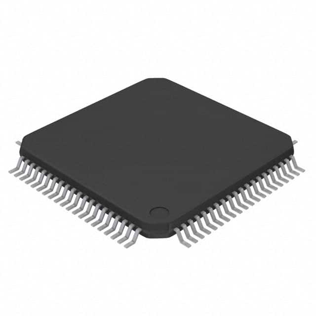
A40MX04-3VQG80 is available in a Quad Flat Pack (QFP) package.
Essence
The essence of A40MX04-3VQG80 lies in its ability to provide a customizable and reconfigurable digital circuit platform, enabling rapid prototyping and development of various electronic systems.
Packaging/Quantity
This product is typically sold in reels or trays containing a specific quantity of units. The exact packaging and quantity may vary depending on the supplier.
Specifications
- Device Type: FPGA
- Family: A40MX
- Number of Logic Cells: 4,000
- Number of I/O Pins: 80
- Operating Voltage: 3.3V
- Package Type: QFP
- Package Size: 14mm x 14mm
Detailed Pin Configuration
The pin configuration of A40MX04-3VQG80 is as follows:
(Please refer to the datasheet or manufacturer's documentation for the detailed pin configuration.)
Functional Features
- High-speed performance: A40MX04-3VQG80 offers fast processing capabilities, making it suitable for applications requiring real-time data processing.
- Programmability: The FPGA can be programmed using Hardware Description Languages (HDLs) such as VHDL or Verilog, allowing for the implementation of complex digital circuits.
- I/O Flexibility: This FPGA provides a sufficient number of I/O pins to interface with external devices and peripherals.
- Embedded Memory: A40MX04-3VQG80 includes embedded memory blocks that can be used for storing data or implementing memory-intensive functions.
Advantages and Disadvantages
Advantages
- Flexibility: FPGAs offer flexibility in terms of circuit design and reconfiguration, enabling rapid prototyping and customization.
- High Integration: A40MX04-3VQG80 allows for the integration of multiple digital circuits on a single chip, reducing the overall system complexity.
- Time-to-Market: With FPGAs, designers can quickly develop and test their digital systems, reducing the time required for product development.
Disadvantages
- Power Consumption: FPGAs tend to consume more power compared to application-specific integrated circuits (ASICs).
- Complexity: Designing complex circuits on an FPGA requires expertise in hardware description languages and digital design principles.
Working Principles
A40MX04-3VQG80 operates based on the principle of configurable logic blocks (CLBs) and programmable interconnects. CLBs consist of look-up tables (LUTs), flip-flops, and other components that can be configured to implement desired logic functions. The programmable interconnects allow for the routing of signals between different CLBs, enabling the creation of complex digital circuits.
Detailed Application Field Plans
A40MX04-3VQG80 finds applications in various fields, including: 1. Telecommunications: Used in the development of communication systems, such as network routers and switches. 2. Industrial Automation: Employed in control systems for industrial machinery and robotics. 3. Automotive Electronics: Utilized in automotive applications, including engine control units (ECUs) and advanced driver-assistance systems (ADAS). 4. Aerospace and Defense: Used in avionics systems, radar signal processing, and military communication equipment.
Detailed and Complete Alternative Models
Some alternative models to A40MX04-3VQG80 include: 1. A40MX02-PLG68: Offers a lower number of logic cells and I/O pins but provides a cost-effective solution for less complex designs. 2. A40MX09-FPLG84: Provides a higher number of logic cells and I/O pins, suitable for more demanding applications. 3. A40MX16-PQG100: Offers increased capacity with 16,000 logic cells, enabling the implementation of larger and more complex digital circuits.
These alternative models cater to different design requirements and can be chosen based on the specific needs of the project.
(Note: The content provided above is a general outline and may require further expansion and refinement to reach
10个与A40MX04-3VQG80在技术解决方案中的应用相关的常见问题及解答
Sure! Here are 10 common questions and answers related to the application of A40MX04-3VQG80 in technical solutions:
Question: What is the A40MX04-3VQG80?
Answer: The A40MX04-3VQG80 is a specific model of field-programmable gate array (FPGA) manufactured by Microsemi.Question: What are the key features of the A40MX04-3VQG80?
Answer: The A40MX04-3VQG80 features 4,000 logic cells, 80 I/O pins, and operates at a voltage of 3.3V.Question: In what applications can the A40MX04-3VQG80 be used?
Answer: The A40MX04-3VQG80 can be used in various applications such as telecommunications, industrial automation, medical devices, and aerospace systems.Question: How can the A40MX04-3VQG80 be programmed?
Answer: The A40MX04-3VQG80 can be programmed using hardware description languages (HDLs) like VHDL or Verilog, or through graphical programming tools provided by the manufacturer.Question: Can the A40MX04-3VQG80 be reprogrammed after deployment?
Answer: Yes, the A40MX04-3VQG80 is a reprogrammable FPGA, allowing for flexibility and updates to the design even after deployment.Question: What is the maximum operating frequency of the A40MX04-3VQG80?
Answer: The maximum operating frequency of the A40MX04-3VQG80 depends on the specific design and implementation, but it can typically reach frequencies in the range of tens to hundreds of megahertz.Question: Does the A40MX04-3VQG80 support external memory interfaces?
Answer: Yes, the A40MX04-3VQG80 supports various external memory interfaces such as SDRAM, SRAM, and Flash memory.Question: Can the A40MX04-3VQG80 interface with other digital or analog components?
Answer: Yes, the A40MX04-3VQG80 can interface with other digital components through its I/O pins, and with analog components using appropriate interface circuitry.Question: What is the power consumption of the A40MX04-3VQG80?
Answer: The power consumption of the A40MX04-3VQG80 depends on the specific design and utilization, but it typically operates within a low-power range suitable for many applications.Question: Are there any development tools or resources available for working with the A40MX04-3VQG80?
Answer: Yes, Microsemi provides development tools, documentation, and support for designing and programming with the A40MX04-3VQG80 FPGA. These resources can be accessed through their official website.