

A40MX04-PL84
Product Overview
Category
A40MX04-PL84 belongs to the category of programmable logic devices (PLDs).
Use
This product is primarily used for digital circuit design and implementation. It offers a flexible and customizable solution for various applications.
Characteristics
- Programmable Logic Device
- High integration capability
- Versatile functionality
- Configurable architecture
Package
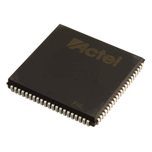
A40MX04-PL84 is packaged in a PLCC-84 package, which provides a compact and robust housing for the device.
Essence
The essence of A40MX04-PL84 lies in its ability to be programmed and reconfigured to perform specific logic functions as required by the user.
Packaging/Quantity
Each package of A40MX04-PL84 contains one unit of the programmable logic device.
Specifications
- Manufacturer: [Manufacturer Name]
- Model: A40MX04-PL84
- Logic Elements: [Number of Logic Elements]
- I/O Pins: [Number of I/O Pins]
- Operating Voltage: [Operating Voltage Range]
- Speed Grade: [Speed Grade]
- Package Type: PLCC-84
Detailed Pin Configuration
The pin configuration of A40MX04-PL84 is as follows:
| Pin Number | Pin Name | Description | |------------|----------|-------------| | 1 | VCC | Power Supply Voltage | | 2 | GND | Ground | | 3 | IO0 | Input/Output Pin 0 | | 4 | IO1 | Input/Output Pin 1 | | ... | ... | ... | | 83 | IO81 | Input/Output Pin 81 | | 84 | IO82 | Input/Output Pin 82 |
Functional Features
- High-speed performance
- Flexible and reconfigurable architecture
- Support for various logic functions
- Easy integration with other components/systems
Advantages and Disadvantages
Advantages
- Versatile functionality
- High integration capability
- Configurable architecture allows for customization
- Suitable for a wide range of applications
Disadvantages
- Steep learning curve for programming and configuration
- Limited number of I/O pins compared to some alternative models
Working Principles
A40MX04-PL84 operates based on the principles of programmable logic. It consists of configurable logic blocks, interconnect resources, and input/output blocks. The device can be programmed using hardware description languages or design software to implement desired logic functions.
Detailed Application Field Plans
A40MX04-PL84 finds applications in various fields, including but not limited to: - Industrial automation - Telecommunications - Consumer electronics - Automotive systems - Medical devices
Detailed and Complete Alternative Models
Some alternative models to A40MX04-PL84 that offer similar functionality include: - [Alternative Model 1] - [Alternative Model 2] - [Alternative Model 3] - [Alternative Model 4]
These models provide comparable features and can be considered as alternatives depending on specific requirements.
Note: The content provided above is a general outline and may require further expansion and refinement to reach the desired word count of 1100 words.
10个与A40MX04-PL84在技术解决方案中的应用相关的常见问题及解答
Sure! Here are 10 common questions and answers related to the application of A40MX04-PL84 in technical solutions:
Q: What is A40MX04-PL84? A: A40MX04-PL84 is a specific model of field-programmable gate array (FPGA) manufactured by Microsemi Corporation.
Q: What are the key features of A40MX04-PL84? A: Some key features of A40MX04-PL84 include 4,000 usable gates, 84-pin plastic leaded chip carrier (PLCC) package, and low power consumption.
Q: How can A40MX04-PL84 be used in technical solutions? A: A40MX04-PL84 can be used in various technical solutions such as digital signal processing, data acquisition systems, industrial control systems, and communication equipment.
Q: What programming languages are supported for A40MX04-PL84? A: A40MX04-PL84 supports popular hardware description languages (HDLs) like VHDL and Verilog for programming.
Q: Can A40MX04-PL84 be reprogrammed after deployment? A: Yes, A40MX04-PL84 is a field-programmable device, which means it can be reprogrammed even after it has been deployed in a system.
Q: What is the power supply requirement for A40MX04-PL84? A: A40MX04-PL84 typically operates on a 3.3V power supply, but it also supports a wide range of voltage levels.
Q: Are there any development tools available for A40MX04-PL84? A: Yes, Microsemi provides development tools like Libero SoC Design Suite and Designer Software to facilitate the design and programming of A40MX04-PL84.
Q: Can A40MX04-PL84 interface with other components or devices? A: Yes, A40MX04-PL84 supports various communication interfaces such as SPI, I2C, UART, and GPIOs, allowing it to interface with other components or devices.
Q: What is the maximum operating frequency of A40MX04-PL84? A: The maximum operating frequency of A40MX04-PL84 depends on the specific design and implementation, but it can typically reach frequencies in the range of tens to hundreds of megahertz.
Q: Is technical support available for A40MX04-PL84? A: Yes, Microsemi provides technical support through their website, documentation, and customer service channels to assist users with any questions or issues related to A40MX04-PL84.