

A42MX09-FVQG100
Product Overview
Category
The A42MX09-FVQG100 belongs to the category of Field Programmable Gate Arrays (FPGAs).
Use
This FPGA is designed for use in various electronic applications that require programmable logic devices.
Characteristics
- The A42MX09-FVQG100 offers high-performance and flexibility due to its programmable nature.
- It has a compact size, making it suitable for space-constrained designs.
- This FPGA supports a wide range of I/O standards, enabling compatibility with different interfaces.
- It operates at low power consumption levels, making it energy-efficient.
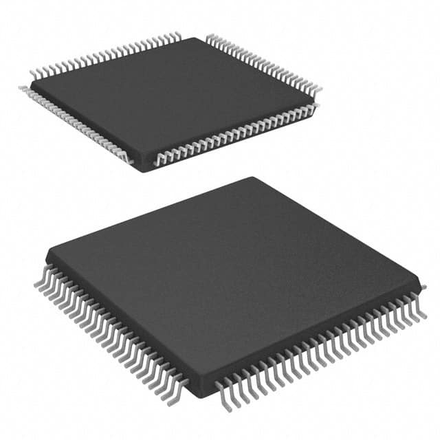
Package
The A42MX09-FVQG100 comes in a standard quad flat package (QFP), which ensures easy integration into circuit boards.
Essence
The essence of the A42MX09-FVQG100 lies in its ability to provide reconfigurable logic functions, allowing users to implement custom digital circuits.
Packaging/Quantity
Each package contains one A42MX09-FVQG100 FPGA.
Specifications
- Logic Elements: 9,600
- Maximum Frequency: 200 MHz
- Embedded Memory: 288 Kbits
- I/O Pins: 100
- Operating Voltage: 3.3V
- Package Type: QFP
- Temperature Range: -40°C to +85°C
Detailed Pin Configuration
The A42MX09-FVQG100 has a total of 100 pins, each serving a specific purpose. The detailed pin configuration can be found in the product datasheet.
Functional Features
- High-speed performance: The FPGA operates at a maximum frequency of 200 MHz, enabling rapid data processing.
- Reconfigurability: Users can modify the logic functions of the FPGA as per their requirements, providing flexibility in design.
- Embedded memory: The FPGA includes 288 Kbits of embedded memory, allowing for efficient data storage and retrieval.
- I/O compatibility: With support for various I/O standards, the FPGA can interface with a wide range of devices.
Advantages and Disadvantages
Advantages
- Flexibility in design due to reconfigurability.
- High-performance capabilities.
- Compact size for space-constrained applications.
- Low power consumption, resulting in energy efficiency.
Disadvantages
- Limited logic elements compared to higher-end FPGAs.
- Relatively smaller embedded memory capacity.
Working Principles
The A42MX09-FVQG100 operates based on the principles of configurable logic. It consists of programmable logic blocks interconnected through configurable routing resources. Users can program the FPGA using hardware description languages (HDL) or specialized software tools. Once programmed, the FPGA executes the desired logic functions by configuring its internal circuitry.
Detailed Application Field Plans
The A42MX09-FVQG100 finds applications in various fields, including: 1. Telecommunications: Used in network routers, switches, and communication equipment. 2. Industrial Automation: Employed in control systems, robotics, and process automation. 3. Automotive Electronics: Integrated into automotive control units, infotainment systems, and driver assistance systems. 4. Consumer Electronics: Utilized in smart TVs, gaming consoles, and home automation devices. 5. Medical Devices: Incorporated into medical imaging equipment, patient monitoring systems, and diagnostic instruments.
Detailed and Complete Alternative Models
A42MX16-FPQG208
- Logic Elements: 16,000
- Maximum Frequency: 250 MHz
- Embedded Memory: 576 Kbits
- I/O Pins: 208
- Operating Voltage: 3.3V
- Package Type: QFP
- Temperature Range: -40°C to +85°C
A42MX24-FPQG240
- Logic Elements: 24,000
- Maximum Frequency: 300 MHz
- Embedded Memory: 1,152 Kbits
- I/O Pins: 240
- Operating Voltage: 3.3V
- Package Type: QFP
- Temperature Range: -40°C to +85°C
A42MX36-FPQG352
- Logic Elements: 36,000
- Maximum Frequency: 350 MHz
- Embedded Memory: 1,728 Kbits
- I/O Pins: 352
- Operating Voltage: 3.3V
- Package Type: QFP
- Temperature Range: -40°C to +85°C
A42MX49-FPQG480
- Logic Elements: 49,000
- Maximum Frequency: 400 MHz
- Embedded Memory: 2,304 Kbits
- I/O Pins: 480
10个与A42MX09-FVQG100在技术解决方案中的应用相关的常见问题及解答
Sure! Here are 10 common questions and answers related to the application of A42MX09-FVQG100 in technical solutions:
Question: What is the A42MX09-FVQG100?
Answer: The A42MX09-FVQG100 is a specific model of field-programmable gate array (FPGA) manufactured by Microsemi.Question: What are the key features of the A42MX09-FVQG100?
Answer: Some key features include 9,216 logic elements, 288 I/O pins, 4 global clock networks, and 100-pin FineLine BGA package.Question: What are the typical applications for the A42MX09-FVQG100?
Answer: The A42MX09-FVQG100 is commonly used in various technical solutions such as telecommunications, industrial automation, medical devices, and aerospace systems.Question: How can I program the A42MX09-FVQG100?
Answer: The A42MX09-FVQG100 can be programmed using hardware description languages (HDLs) like VHDL or Verilog, along with appropriate development tools provided by Microsemi.Question: Can the A42MX09-FVQG100 be reprogrammed after deployment?
Answer: Yes, the A42MX09-FVQG100 is a reprogrammable FPGA, allowing for flexibility and updates even after it has been deployed in a system.Question: What is the power consumption of the A42MX09-FVQG100?
Answer: The power consumption of the A42MX09-FVQG100 varies depending on the specific design and usage, but it is generally designed to be power-efficient.Question: Are there any specific design considerations when using the A42MX09-FVQG100?
Answer: Yes, it is important to consider factors such as clock frequency, I/O requirements, power supply, and thermal management while designing with the A42MX09-FVQG100.Question: Can the A42MX09-FVQG100 interface with other components or devices?
Answer: Yes, the A42MX09-FVQG100 has a wide range of I/O pins that can be used to interface with other components or devices in a system.Question: Does the A42MX09-FVQG100 support communication protocols like Ethernet or USB?
Answer: Yes, the A42MX09-FVQG100 can be programmed to support various communication protocols including Ethernet, USB, SPI, I2C, and more.Question: Where can I find additional resources or support for the A42MX09-FVQG100?
Answer: Microsemi provides documentation, application notes, and technical support for the A42MX09-FVQG100 on their official website. Additionally, online forums and communities dedicated to FPGA development can also be helpful sources of information.