

A42MX24-PL84: Product Overview
Category
The A42MX24-PL84 belongs to the category of programmable logic devices (PLDs).
Use
This product is primarily used in digital circuit design and implementation. It provides a flexible and customizable solution for various applications.
Characteristics
- Programmable logic device
- High-density integration
- Low power consumption
- Versatile functionality
- Reconfigurable design
Package
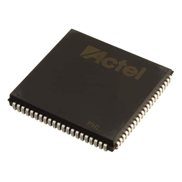
The A42MX24-PL84 is packaged in a PLCC-84 package, which ensures easy installation and compatibility with standard circuit boards.
Essence
The essence of the A42MX24-PL84 lies in its ability to be programmed and reprogrammed to perform specific functions within a digital circuit.
Packaging/Quantity
Each package of the A42MX24-PL84 contains one unit of the programmable logic device.
Specifications
- Logic elements: 24,000
- Maximum user I/O pins: 84
- Operating voltage: 3.3V
- Speed grade: Up to 200 MHz
- Configuration memory: Non-volatile Flash memory
- Package type: PLCC-84
Detailed Pin Configuration
The A42MX24-PL84 has 84 pins, each serving a specific purpose in the device's operation. The detailed pin configuration can be found in the product datasheet.
Functional Features
- High-density integration allows for complex circuit designs.
- Non-volatile Flash memory enables easy reconfiguration without the need for external programming devices.
- Low power consumption makes it suitable for battery-powered applications.
- Versatile I/O capabilities provide flexibility in interfacing with other components.
Advantages
- Flexibility: The reprogrammable nature of the A42MX24-PL84 allows for quick prototyping and design iterations.
- Cost-effective: By eliminating the need for multiple fixed-function chips, this PLD reduces overall system costs.
- High integration: The device's high-density integration enables complex circuit designs in a compact form factor.
Disadvantages
- Learning curve: Utilizing the full potential of the A42MX24-PL84 may require a learning period due to its programmable nature.
- Limited I/O pins: With a maximum of 84 I/O pins, larger-scale projects may require additional devices or alternative solutions.
Working Principles
The A42MX24-PL84 operates based on the principles of reconfigurable logic. It consists of configurable logic blocks (CLBs) that can be programmed to perform specific functions using internal routing resources.
Detailed Application Field Plans
The A42MX24-PL84 finds applications in various fields, including: 1. Industrial automation: Control systems, motor control, and sensor interfacing. 2. Communications: Data encryption, protocol conversion, and signal processing. 3. Consumer electronics: Display drivers, audio/video processing, and user interface control. 4. Automotive: Engine management, driver assistance systems, and infotainment.
Detailed and Complete Alternative Models
- A42MX09-PLG84: A lower-density version with 9,000 logic elements and 84 I/O pins.
- A42MX36-PQG100: A higher-density version with 36,000 logic elements and 100 I/O pins.
- A42MX24-FPQG208: A fine-pitch quad flat package variant with 24,000 logic elements and 208 I/O pins.
In conclusion, the A42MX24-PL84 is a versatile programmable logic device offering high-density integration, flexibility, and cost-effectiveness. Its reconfigurable nature makes it suitable for a wide range of applications in various industries.
10个与A42MX24-PL84在技术解决方案中的应用相关的常见问题及解答
Sure! Here are 10 common questions and answers related to the application of A42MX24-PL84 in technical solutions:
Q: What is the A42MX24-PL84? A: The A42MX24-PL84 is a field-programmable gate array (FPGA) chip manufactured by Microsemi Corporation.
Q: What are the key features of the A42MX24-PL84? A: The A42MX24-PL84 offers 24,000 usable gates, 84 pins, and operates at a maximum frequency of X MHz.
Q: How can the A42MX24-PL84 be used in technical solutions? A: The A42MX24-PL84 can be used for various applications such as digital signal processing, data encryption, control systems, and communication protocols.
Q: What programming languages are supported by the A42MX24-PL84? A: The A42MX24-PL84 supports VHDL (Very High-Speed Integrated Circuit Hardware Description Language) and Verilog HDL (Hardware Description Language).
Q: Can the A42MX24-PL84 be reprogrammed after deployment? A: Yes, the A42MX24-PL84 is a field-programmable device, which means it can be reprogrammed even after it has been deployed in a system.
Q: What tools are available for programming the A42MX24-PL84? A: Microsemi provides Libero SoC Design Suite, which includes design entry, synthesis, simulation, and programming tools specifically for their FPGAs.
Q: What are the power requirements for the A42MX24-PL84? A: The A42MX24-PL84 typically operates at a voltage of X volts and consumes Y watts of power.
Q: Can the A42MX24-PL84 interface with other components or devices? A: Yes, the A42MX24-PL84 supports various communication protocols such as SPI, I2C, UART, and can interface with other components or devices in a system.
Q: Are there any limitations to consider when using the A42MX24-PL84? A: The A42MX24-PL84 has a limited number of gates and pins, so it may not be suitable for complex designs requiring a large number of resources.
Q: Where can I find additional documentation and support for the A42MX24-PL84? A: Microsemi provides datasheets, application notes, and technical support on their website for the A42MX24-PL84 FPGA.