

A54SX08-2FGG144
Product Overview
Category
A54SX08-2FGG144 belongs to the category of Field Programmable Gate Arrays (FPGAs).
Use
This product is primarily used in digital logic circuits for various applications such as telecommunications, automotive, industrial control systems, and consumer electronics.
Characteristics
- High-performance programmable logic device
- Offers flexibility and reconfigurability
- Provides high-speed data processing capabilities
- Supports complex digital designs
- Low power consumption
- Reliable and durable
Package
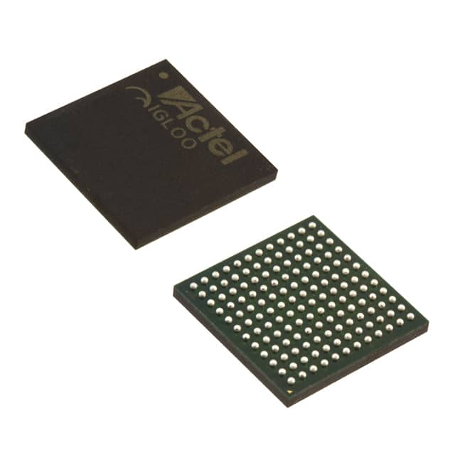
The A54SX08-2FGG144 FPGA comes in a 144-pin Fine-Pitch Ball Grid Array (FBGA) package.
Essence
The essence of this product lies in its ability to provide a customizable and versatile solution for implementing complex digital logic designs.
Packaging/Quantity
Each package contains one A54SX08-2FGG144 FPGA.
Specifications
- Logic Elements: 8,000
- Flip-Flops: 8,000
- Embedded Multiplier Blocks: 16
- Maximum Frequency: 250 MHz
- I/O Pins: 144
- Operating Voltage: 1.5V
- Operating Temperature Range: -40°C to +85°C
Detailed Pin Configuration
The A54SX08-2FGG144 FPGA has a total of 144 pins, each serving a specific purpose in the circuit design. The pin configuration includes input/output pins, power supply pins, ground pins, and configuration pins. For a detailed pin configuration diagram, please refer to the manufacturer's datasheet.
Functional Features
- Configurable logic blocks for implementing custom digital circuits
- Dedicated memory blocks for storing data
- Built-in arithmetic functions and mathematical operations
- Clock management resources for precise timing control
- Flexible I/O interfaces for seamless integration with external devices
- On-chip configuration memory for easy reprogramming
Advantages and Disadvantages
Advantages
- High flexibility and reconfigurability
- Fast data processing capabilities
- Low power consumption
- Reliable performance
- Suitable for a wide range of applications
Disadvantages
- Steep learning curve for beginners
- Limited resources compared to larger FPGAs
- Higher cost compared to other programmable logic devices
Working Principles
The A54SX08-2FGG144 FPGA operates based on the principles of configurable logic. It consists of an array of programmable logic blocks interconnected through configurable routing resources. The user can program the FPGA using Hardware Description Languages (HDLs) such as VHDL or Verilog to define the desired digital circuit functionality. Once programmed, the FPGA executes the logic operations based on the provided configuration.
Detailed Application Field Plans
The A54SX08-2FGG144 FPGA finds applications in various fields, including:
- Telecommunications: Used in network routers, switches, and communication protocols.
- Automotive: Employed in automotive control systems, driver assistance systems, and infotainment systems.
- Industrial Control Systems: Utilized in programmable logic controllers (PLCs), factory automation, and robotics.
- Consumer Electronics: Integrated into high-definition televisions, gaming consoles, and multimedia devices.
Detailed and Complete Alternative Models
- A54SX16A-2FGG144: Offers higher logic capacity with 16,000 logic elements.
- A54SX32A-2FGG144: Provides even greater logic capacity with 32,000 logic elements.
- A54SX64A-2FGG144: Features the highest logic capacity with 64,000 logic elements.
These alternative models offer increased resources and capabilities for more complex digital designs.
Word count: 536
10个与A54SX08-2FGG144在技术解决方案中的应用相关的常见问题及解答
Sure! Here are 10 common questions and answers related to the application of A54SX08-2FGG144 in technical solutions:
Q: What is A54SX08-2FGG144? A: A54SX08-2FGG144 is a specific model of field-programmable gate array (FPGA) manufactured by Microsemi Corporation.
Q: What are the key features of A54SX08-2FGG144? A: Some key features of A54SX08-2FGG144 include 54,000 system gates, 8,192 macrocells, 144-pin FineLine BGA package, and support for various I/O standards.
Q: In what applications can A54SX08-2FGG144 be used? A: A54SX08-2FGG144 can be used in a wide range of applications such as telecommunications, industrial automation, medical devices, aerospace, and defense.
Q: How can I program A54SX08-2FGG144? A: A54SX08-2FGG144 can be programmed using hardware description languages (HDLs) like VHDL or Verilog, and the programming can be done using specialized software tools provided by Microsemi.
Q: Can A54SX08-2FGG144 be reprogrammed after deployment? A: Yes, A54SX08-2FGG144 is a reprogrammable FPGA, which means it can be reconfigured with new designs even after it has been deployed in a system.
Q: What are the power requirements for A54SX08-2FGG144? A: The power requirements for A54SX08-2FGG144 depend on the specific design and usage scenario. It typically operates at a voltage range of 3.3V, but it's important to refer to the datasheet for detailed power specifications.
Q: Does A54SX08-2FGG144 support high-speed interfaces? A: Yes, A54SX08-2FGG144 supports various high-speed interfaces such as LVDS, DDR, and PCI Express, making it suitable for applications that require fast data transfer rates.
Q: Can A54SX08-2FGG144 interface with other components or microcontrollers? A: Yes, A54SX08-2FGG144 can interface with other components or microcontrollers using standard protocols like SPI, I2C, UART, or custom communication interfaces implemented in the FPGA design.
Q: Are there any development boards available for A54SX08-2FGG144? A: Yes, Microsemi provides development boards specifically designed for A54SX08-2FGG144, which include necessary connectors, peripherals, and programming interfaces for easy prototyping and testing.
Q: Where can I find technical documentation and support for A54SX08-2FGG144? A: You can find technical documentation, datasheets, application notes, and support resources for A54SX08-2FGG144 on the official website of Microsemi Corporation or by contacting their customer support team.
Please note that the answers provided here are general and may vary depending on specific requirements and use cases.