

A54SX16A-2TQ144I
Product Overview
Category
The A54SX16A-2TQ144I belongs to the category of Field Programmable Gate Arrays (FPGAs).
Use
FPGAs are integrated circuits that can be programmed and reprogrammed to perform various digital functions. The A54SX16A-2TQ144I is specifically designed for applications requiring high-performance and low-power consumption.
Characteristics
- High-performance FPGA with low power consumption
- Programmable and reprogrammable functionality
- Suitable for a wide range of applications
- Compact package size
- Robust design for reliable operation
Package
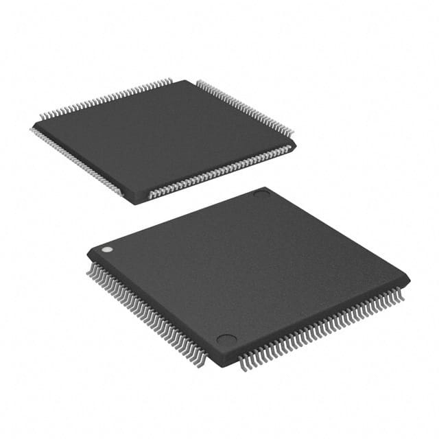
The A54SX16A-2TQ144I comes in a TQFP (Thin Quad Flat Pack) package, which provides ease of handling and compatibility with standard PCB manufacturing processes.
Essence
The essence of the A54SX16A-2TQ144I lies in its ability to provide flexible and customizable digital logic functions, enabling designers to implement complex systems on a single chip.
Packaging/Quantity
The A54SX16A-2TQ144I is typically packaged in reels or trays, with each reel or tray containing a specific quantity of chips. The exact packaging and quantity may vary depending on the supplier.
Specifications
- Logic Elements: 16,000
- Maximum Frequency: 300 MHz
- Embedded Memory: 1,024 Kbits
- I/O Pins: 144
- Operating Voltage: 1.8V - 3.3V
- Package Type: TQFP
- Temperature Range: -40°C to +85°C
Detailed Pin Configuration
The A54SX16A-2TQ144I has 144 pins, each serving a specific purpose in the overall functionality of the FPGA. The pin configuration includes input/output pins, power supply pins, clock pins, and configuration pins. For a detailed pin configuration diagram, please refer to the manufacturer's datasheet.
Functional Features
- High-performance digital logic processing
- Configurable I/O interfaces for versatile connectivity options
- On-chip memory for efficient data storage and retrieval
- Built-in clock management resources for precise timing control
- Support for various communication protocols and standards
- Flexible design architecture allowing for easy customization
Advantages and Disadvantages
Advantages
- Versatile and customizable functionality
- High-performance computing capabilities
- Low power consumption
- Compact package size
- Wide temperature range for operation
Disadvantages
- Steep learning curve for beginners
- Limited availability of technical support for complex designs
- Higher cost compared to traditional fixed-function integrated circuits
Working Principles
The A54SX16A-2TQ144I operates based on the principles of reconfigurable digital logic. It consists of an array of programmable logic elements interconnected through configurable routing resources. The user can program the FPGA using hardware description languages (HDL) or graphical tools to define the desired digital logic functions and interconnections. Once programmed, the FPGA executes the specified logic operations, enabling the implementation of complex digital systems.
Detailed Application Field Plans
The A54SX16A-2TQ144I finds applications in various fields that require high-performance digital processing capabilities. Some potential application areas include:
- Telecommunications: FPGA-based solutions for signal processing, network infrastructure, and wireless communication systems.
- Industrial Automation: Control systems, robotics, and machine vision applications.
- Automotive: Advanced driver assistance systems (ADAS), infotainment systems, and engine control units (ECUs).
- Aerospace and Defense: Radar systems, avionics, and secure communications.
- Medical Devices: Imaging systems, patient monitoring, and diagnostic equipment.
Detailed and Complete Alternative Models
- A54SX32A-2TQ144I: Similar to the A54SX16A-2TQ144I but with double the logic elements (32,000).
- A54SX08A-2TQ144I: A lower-cost alternative with reduced logic elements (8,000) but similar features.
- A54SX04A-2TQ144I: Entry-level FPGA with 4,000 logic elements, suitable for smaller-scale applications.
Note: The above alternative models are provided as examples and may vary depending on the manufacturer's product lineup.
Word count: 609 words
10个与A54SX16A-2TQ144I在技术解决方案中的应用相关的常见问题及解答
Sure! Here are 10 common questions and answers related to the application of A54SX16A-2TQ144I in technical solutions:
Question: What is the A54SX16A-2TQ144I?
Answer: The A54SX16A-2TQ144I is a specific model of field-programmable gate array (FPGA) manufactured by Microsemi.Question: What are the key features of the A54SX16A-2TQ144I?
Answer: Some key features include 54,000 system gates, 16,000 usable gates, 144-pin TQFP package, and support for various I/O standards.Question: In what technical solutions can the A54SX16A-2TQ144I be used?
Answer: The A54SX16A-2TQ144I can be used in a wide range of applications such as telecommunications, industrial automation, medical devices, and aerospace systems.Question: How does the A54SX16A-2TQ144I benefit telecommunications applications?
Answer: It provides high-speed data processing capabilities, supports various communication protocols, and enables efficient signal processing for tasks like voice and video transmission.Question: Can the A54SX16A-2TQ144I be used in industrial automation systems?
Answer: Yes, it can be used for tasks like control logic implementation, sensor interfacing, and real-time monitoring in industrial automation applications.Question: What advantages does the A54SX16A-2TQ144I offer in medical devices?
Answer: It allows for complex algorithm implementation, precise control of medical equipment, and integration with other components for advanced medical diagnostics.Question: Is the A54SX16A-2TQ144I suitable for aerospace systems?
Answer: Yes, it is suitable for aerospace applications due to its radiation-hardened design, reliability in harsh environments, and ability to handle complex calculations.Question: Can the A54SX16A-2TQ144I be programmed by users?
Answer: Yes, it is a field-programmable device, meaning users can configure its functionality using hardware description languages like VHDL or Verilog.Question: What are the power requirements for the A54SX16A-2TQ144I?
Answer: It typically operates at a voltage range of 3.3V, but specific power requirements may vary depending on the application and system design.Question: Are there any development tools available for working with the A54SX16A-2TQ144I?
Answer: Yes, Microsemi provides development tools such as Libero SoC Design Suite, which includes software for designing, simulating, and programming the FPGA.
Please note that these questions and answers are general and may vary based on specific requirements and applications.