

A54SX16A-2TQG144I
Product Overview
Category
The A54SX16A-2TQG144I belongs to the category of Field Programmable Gate Arrays (FPGAs).
Use
FPGAs are integrated circuits that can be programmed and reprogrammed to perform various digital functions. The A54SX16A-2TQG144I is specifically designed for applications requiring high-performance and low-power consumption.
Characteristics
- High-performance FPGA with low power consumption
- Flexible and reprogrammable design
- Suitable for a wide range of applications
- Compact package for easy integration
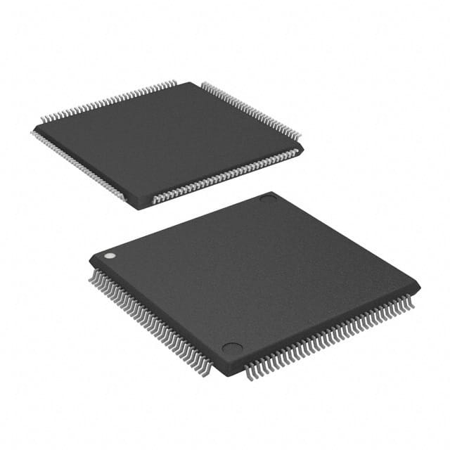
Package
The A54SX16A-2TQG144I comes in a 144-pin Thin Quad Flat Pack (TQFP) package.
Essence
The essence of the A54SX16A-2TQG144I lies in its ability to provide customizable digital functionality in a compact and efficient manner.
Packaging/Quantity
The A54SX16A-2TQG144I is typically packaged individually and is available in various quantities depending on the manufacturer's specifications.
Specifications
- Number of Logic Cells: 16,000
- Number of I/O Pins: 54
- Operating Voltage: 1.8V
- Maximum Frequency: 400 MHz
- Programmable Logic Blocks: 1,600
- Embedded Memory: 576 Kbits
- On-Chip PLLs: 4
- Configuration Bits: 1,000,000
Detailed Pin Configuration
The A54SX16A-2TQG144I has a total of 144 pins. These pins are assigned to various functions such as input/output, power supply, configuration, and clock signals. The detailed pin configuration can be found in the product datasheet provided by the manufacturer.
Functional Features
- High-performance digital signal processing
- Flexible and reprogrammable logic design
- Low power consumption
- On-chip PLLs for clock management
- Embedded memory for data storage
- Support for various communication protocols
Advantages and Disadvantages
Advantages
- Customizable functionality to meet specific application requirements
- High-performance processing capabilities
- Low power consumption for energy-efficient operation
- Compact package for easy integration into existing systems
- Support for a wide range of communication protocols
Disadvantages
- Complexity in programming and configuration
- Limited availability of alternative models with similar specifications
- Higher cost compared to standard microcontrollers or ASICs
Working Principles
The A54SX16A-2TQG144I works based on the principles of digital logic design. It consists of programmable logic blocks, embedded memory, and input/output pins. The FPGA can be programmed using Hardware Description Languages (HDL) such as VHDL or Verilog to define the desired functionality. Once programmed, the FPGA executes the logic functions and processes the incoming data according to the defined configuration.
Detailed Application Field Plans
The A54SX16A-2TQG144I finds applications in various fields, including but not limited to:
- Telecommunications: Used in base stations, routers, and network switches for high-speed data processing and protocol handling.
- Industrial Automation: Employed in control systems, robotics, and machine vision applications for real-time data processing and control.
- Aerospace and Defense: Utilized in radar systems, avionics, and military communication equipment for high-performance signal processing and encryption.
- Medical Devices: Integrated into medical imaging systems, patient monitoring devices, and laboratory equipment for data acquisition and analysis.
- Automotive: Applied in advanced driver assistance systems (ADAS), infotainment systems, and engine control units for efficient data processing and control.
Detailed and Complete Alternative Models
While the A54SX16A-2TQG144I offers unique features, there are alternative FPGA models available in the market with similar specifications. Some notable alternatives include:
- Xilinx Spartan-6 XC6SLX16: Offers comparable logic capacity and I/O pin count.
- Intel Cyclone IV EP4CE15: Provides similar performance and power characteristics.
- Lattice Semiconductor iCE40HX1K: Suitable for low-power applications with smaller logic requirements.
These alternative models can be considered based on specific project requirements and availability.
Word count: 539 words
10个与A54SX16A-2TQG144I在技术解决方案中的应用相关的常见问题及解答
Sure! Here are 10 common questions and answers related to the application of A54SX16A-2TQG144I in technical solutions:
Question: What is the A54SX16A-2TQG144I?
Answer: The A54SX16A-2TQG144I is a specific model of programmable logic device (PLD) manufactured by Microsemi.Question: What is the purpose of using A54SX16A-2TQG144I in technical solutions?
Answer: The A54SX16A-2TQG144I is used for implementing complex digital logic functions in various applications, such as telecommunications, industrial control systems, and automotive electronics.Question: What are the key features of A54SX16A-2TQG144I?
Answer: Some key features of A54SX16A-2TQG144I include 16,000 usable gates, 144-pin TQFP package, high-speed performance, and low power consumption.Question: How can I program the A54SX16A-2TQG144I?
Answer: The A54SX16A-2TQG144I can be programmed using industry-standard hardware description languages (HDLs) like VHDL or Verilog, and then configured using appropriate programming tools provided by Microsemi.Question: Can the A54SX16A-2TQG144I be reprogrammed?
Answer: Yes, the A54SX16A-2TQG144I supports in-system programmability, allowing you to reprogram it even after it has been soldered onto a circuit board.Question: What are the voltage requirements for A54SX16A-2TQG144I?
Answer: The A54SX16A-2TQG144I operates at a voltage range of 3.3V, making it compatible with standard digital logic levels.Question: Can the A54SX16A-2TQG144I interface with other components or microcontrollers?
Answer: Yes, the A54SX16A-2TQG144I can interface with other components and microcontrollers using various communication protocols such as SPI, I2C, UART, or custom interfaces.Question: What is the maximum operating frequency of A54SX16A-2TQG144I?
Answer: The maximum operating frequency of A54SX16A-2TQG144I depends on the specific design and implementation, but it can typically reach frequencies in the range of tens to hundreds of megahertz.Question: Are there any development tools available for designing with A54SX16A-2TQG144I?
Answer: Yes, Microsemi provides development tools like Libero SoC Design Suite, which includes software for designing, simulating, and programming the A54SX16A-2TQG144I.Question: Where can I find more information about A54SX16A-2TQG144I and its applications?
Answer: You can refer to the official documentation and datasheets provided by Microsemi, visit their website, or consult application notes and reference designs related to A54SX16A-2TQG144I.