

A54SX16A-TQ100
Product Overview
Category
The A54SX16A-TQ100 belongs to the category of Field-Programmable Gate Arrays (FPGAs).
Use
This product is primarily used in digital logic circuits for various applications such as telecommunications, automotive, industrial automation, and consumer electronics.
Characteristics
- High-performance FPGA with advanced features
- Flexible and reconfigurable design
- Low power consumption
- High-speed data processing capabilities
Package
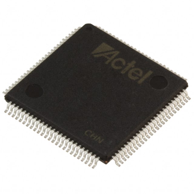
The A54SX16A-TQ100 comes in a TQFP (Thin Quad Flat Pack) package.
Essence
The essence of this product lies in its ability to provide a customizable hardware solution that can be programmed and reprogrammed to perform specific tasks efficiently.
Packaging/Quantity
The A54SX16A-TQ100 is typically packaged in reels or trays, and the quantity per package may vary depending on the supplier.
Specifications
- Logic Elements: 16,000
- Maximum Frequency: 200 MHz
- Embedded Memory: 1,024 Kbits
- I/O Pins: 100
- Operating Voltage: 3.3V
- Package Type: TQFP
- Temperature Range: -40°C to +85°C
Detailed Pin Configuration
The A54SX16A-TQ100 has a total of 100 pins, each serving a specific purpose in the circuit design. The pin configuration includes input/output pins, power supply pins, clock pins, and configuration pins. For a detailed pin configuration diagram, please refer to the product datasheet.
Functional Features
- Configurable logic blocks for implementing complex digital circuits
- Dedicated memory blocks for efficient data storage and retrieval
- Programmable interconnects for flexible routing of signals
- Built-in clock management resources for precise timing control
- Support for various communication protocols and interfaces
Advantages and Disadvantages
Advantages
- High flexibility and reconfigurability
- Faster time-to-market due to programmable nature
- Lower development costs compared to custom ASICs
- Ability to adapt to changing requirements through reprogramming
Disadvantages
- Higher power consumption compared to dedicated hardware solutions
- Limited performance compared to application-specific integrated circuits (ASICs)
- Steeper learning curve for programming and design implementation
Working Principles
The A54SX16A-TQ100 operates based on the principles of digital logic design. It consists of configurable logic blocks, memory elements, interconnect resources, and clock management units. The FPGA can be programmed using a Hardware Description Language (HDL) to define the desired functionality. Upon configuration, the FPGA executes the programmed logic, enabling the desired operations.
Detailed Application Field Plans
The A54SX16A-TQ100 finds applications in various fields, including:
- Telecommunications: Used in base stations, network switches, and routers for signal processing and data handling.
- Automotive: Employed in automotive control systems, driver assistance systems, and infotainment systems.
- Industrial Automation: Utilized in industrial control systems, robotics, and factory automation.
- Consumer Electronics: Integrated into multimedia devices, gaming consoles, and smart home appliances.
Detailed and Complete Alternative Models
- A54SX08A-TQ100: Similar to A54SX16A-TQ100 but with 8,000 logic elements.
- A54SX32A-TQ100: Enhanced version with 32,000 logic elements for more complex designs.
- A54SX64A-TQ100: Higher-end model with 64,000 logic elements for demanding applications.
These alternative models provide varying levels of logic capacity to cater to different project requirements.
In conclusion, the A54SX16A-TQ100 is a versatile FPGA that offers high performance, flexibility, and reconfigurability. It finds applications in diverse fields and can be programmed to meet specific design needs. While it has certain limitations compared to ASICs, its advantages make it an attractive choice for many digital logic circuit designs.
Word count: 540
10个与A54SX16A-TQ100在技术解决方案中的应用相关的常见问题及解答
What is the maximum operating frequency of A54SX16A-TQ100?
- The maximum operating frequency of A54SX16A-TQ100 is 250 MHz.What are the typical applications for A54SX16A-TQ100?
- A54SX16A-TQ100 is commonly used in industrial control, automotive, and consumer electronics applications.What is the power supply voltage range for A54SX16A-TQ100?
- The power supply voltage range for A54SX16A-TQ100 is 3.0V to 3.6V.Can A54SX16A-TQ100 be reprogrammed after initial configuration?
- Yes, A54SX16A-TQ100 supports in-system programming (ISP) for reconfiguration.What type of package does A54SX16A-TQ100 come in?
- A54SX16A-TQ100 is available in a 100-pin TQFP (Thin Quad Flat Pack) package.Does A54SX16A-TQ100 have built-in security features?
- Yes, A54SX16A-TQ100 includes security features such as bitstream encryption and authentication.What is the maximum number of I/O pins on A54SX16A-TQ100?
- A54SX16A-TQ100 has a maximum of 80 I/O pins.Is A54SX16A-TQ100 RoHS compliant?
- Yes, A54SX16A-TQ100 is RoHS compliant, meeting environmental standards.Can A54SX16A-TQ100 interface with external memory devices?
- Yes, A54SX16A-TQ100 supports interfacing with external SRAM, SDRAM, and Flash memory devices.What development tools are available for A54SX16A-TQ100?
- Development tools such as design software, evaluation boards, and programming hardware are available for A54SX16A-TQ100.