

A54SX16A-TQG144
Product Overview
Category
The A54SX16A-TQG144 belongs to the category of Field-Programmable Gate Arrays (FPGAs).
Use
This product is primarily used in digital circuit design and implementation. FPGAs provide a flexible and customizable solution for various applications, including telecommunications, automotive, aerospace, and consumer electronics.
Characteristics
- High integration: The A54SX16A-TQG144 offers a high level of integration, allowing for complex designs to be implemented on a single chip.
- Reconfigurability: FPGAs can be reprogrammed multiple times, enabling rapid prototyping and design iterations.
- Parallel processing: These devices support parallel processing, making them suitable for applications that require high-speed data processing.
- Low power consumption: The A54SX16A-TQG144 is designed to minimize power consumption, making it energy-efficient.
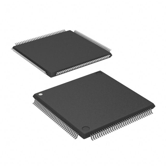
Package and Quantity
The A54SX16A-TQG144 comes in a TQFP (Thin Quad Flat Pack) package. Each package contains one unit of the FPGA.
Specifications
- Number of Logic Cells: 54,000
- Number of I/O Pins: 144
- Operating Voltage: 1.2V
- Maximum Frequency: 400 MHz
- Programmable Logic Blocks: 3,000
- Embedded Memory: 1,080 Kbits
- DSP Slices: 48
Detailed Pin Configuration
The pin configuration of the A54SX16A-TQG144 is as follows:
| Pin Number | Pin Name | Function | |------------|----------|----------| | 1 | VCCINT | Power Supply (Internal) | | 2 | GND | Ground | | 3 | IOB0 | Input/Output Buffer | | ... | ... | ... | | 144 | IOB143 | Input/Output Buffer |
Functional Features
- Configurable Logic Blocks (CLBs): The A54SX16A-TQG144 contains a large number of CLBs that can be programmed to implement various logic functions.
- I/O Interfaces: It provides multiple I/O interfaces, allowing for seamless integration with external devices.
- Clock Management: This FPGA includes dedicated clock management resources, enabling precise control and distribution of clock signals.
- Embedded Memory: The A54SX16A-TQG144 features embedded memory blocks that can be used for data storage or as lookup tables.
Advantages and Disadvantages
Advantages
- Flexibility: FPGAs offer the advantage of reconfigurability, allowing designers to adapt their circuits to changing requirements.
- High Performance: With parallel processing capabilities and high clock frequencies, FPGAs can achieve excellent performance in demanding applications.
- Rapid Prototyping: FPGAs enable quick prototyping and iterative design cycles, reducing time-to-market.
Disadvantages
- Complexity: Designing for FPGAs requires specialized knowledge and expertise, making it more challenging compared to traditional ASIC design.
- Power Consumption: While efforts have been made to reduce power consumption, FPGAs still consume more power compared to application-specific integrated circuits (ASICs).
- Cost: FPGAs tend to be more expensive than off-the-shelf microcontrollers or ASICs, especially for high-capacity devices.
Working Principles
FPGAs consist of an array of configurable logic blocks interconnected by programmable routing resources. The configuration of these blocks and interconnections is determined by the user's design, which is implemented using a hardware description language (HDL) and synthesized into a bitstream. The bitstream is then loaded onto the FPGA, configuring it to perform the desired logic functions.
Detailed Application Field Plans
The A54SX16A-TQG144 can be applied in various fields, including: - Telecommunications: FPGAs are used in base stations, network switches, and routers to handle high-speed data processing and protocol conversion. - Automotive: These devices find applications in automotive electronics for tasks such as engine control, advanced driver-assistance systems (ADAS), and infotainment systems. - Aerospace: FPGAs are utilized in aerospace applications for tasks like satellite communication, radar signal processing, and flight control systems. - Consumer Electronics: They are employed in consumer electronic devices such as gaming consoles, digital cameras, and high-definition televisions for enhanced performance and functionality.
Alternative Models
- A54SX32A-TQG144
- A54SX64A-TQG144
- A54SX128A-TQG144
These alternative models offer higher logic capacity and additional features compared to the A54SX16A-TQG144.
In conclusion, the A54SX16A-TQG144 is a versatile FPGA that provides high integration, reconfigurability, and parallel
10个与A54SX16A-TQG144在技术解决方案中的应用相关的常见问题及解答
Sure! Here are 10 common questions and answers related to the application of A54SX16A-TQG144 in technical solutions:
Question: What is the A54SX16A-TQG144?
Answer: The A54SX16A-TQG144 is a specific model of field-programmable gate array (FPGA) manufactured by Microsemi.Question: What are the key features of the A54SX16A-TQG144?
Answer: Some key features of this FPGA include 54,000 system gates, 16,000 usable gates, 144-pin TQFP package, and support for various I/O standards.Question: What applications can the A54SX16A-TQG144 be used for?
Answer: This FPGA can be used in a wide range of applications such as industrial automation, telecommunications, automotive electronics, medical devices, and more.Question: How can I program the A54SX16A-TQG144?
Answer: The A54SX16A-TQG144 can be programmed using industry-standard hardware description languages (HDLs) like VHDL or Verilog.Question: What development tools are available for working with the A54SX16A-TQG144?
Answer: Microsemi provides a suite of development tools, including Libero SoC Design Suite, which offers synthesis, simulation, and programming capabilities for their FPGAs.Question: Can the A54SX16A-TQG144 be reprogrammed after deployment?
Answer: Yes, FPGAs like the A54SX16A-TQG144 are known for their reprogrammability, allowing for updates and modifications even after deployment.Question: What are the power requirements for the A54SX16A-TQG144?
Answer: The power requirements can vary depending on the specific application and configuration, but typically it operates at a voltage range of 3.3V to 5V.Question: Does the A54SX16A-TQG144 support any communication protocols?
Answer: Yes, this FPGA supports various communication protocols such as SPI, I2C, UART, and CAN, making it suitable for interfacing with other devices.Question: Can the A54SX16A-TQG144 be used in safety-critical applications?
Answer: Yes, Microsemi FPGAs are designed to meet stringent safety standards, making them suitable for use in safety-critical applications like aerospace or medical devices.Question: Are there any reference designs or application notes available for the A54SX16A-TQG144?
Answer: Yes, Microsemi provides reference designs and application notes that can help developers get started with implementing the A54SX16A-TQG144 in their projects.
Please note that the answers provided here are general and may vary based on specific requirements and documentation provided by the manufacturer.