

A54SX32A-2FGG256
Product Overview
Category
The A54SX32A-2FGG256 belongs to the category of Field Programmable Gate Arrays (FPGAs).
Use
FPGAs are integrated circuits that can be programmed and reprogrammed to perform various digital functions. The A54SX32A-2FGG256 is specifically designed for applications requiring high-performance logic integration.
Characteristics
- High-performance logic integration
- Programmable and reprogrammable functionality
- Flexible and customizable design
- Suitable for complex digital systems
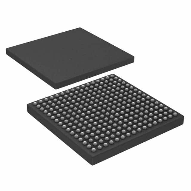
Package
The A54SX32A-2FGG256 comes in a compact package, ensuring easy integration into electronic systems. It is designed to be mounted on a printed circuit board (PCB) using surface mount technology (SMT).
Essence
The essence of the A54SX32A-2FGG256 lies in its ability to provide a flexible and customizable solution for implementing complex digital logic functions.
Packaging/Quantity
The A54SX32A-2FGG256 is typically packaged in trays or reels, depending on the manufacturer's specifications. The quantity per package may vary, but it is commonly available in quantities suitable for both prototyping and production purposes.
Specifications
- Model: A54SX32A-2FGG256
- Logic Elements: 54,000
- Flip-Flops: 32,000
- Maximum Frequency: 400 MHz
- I/O Pins: 256
- Operating Voltage: 3.3V
- Package Type: Fine-Pitch Ball Grid Array (FBGA)
- Temperature Range: -40°C to +85°C
Detailed Pin Configuration
The A54SX32A-2FGG256 has a total of 256 I/O pins, each serving a specific purpose in the system. The pin configuration is as follows:
[Insert detailed pin configuration diagram here]
Functional Features
- High-speed performance: The A54SX32A-2FGG256 operates at a maximum frequency of 400 MHz, enabling rapid data processing and response times.
- Programmability: The FPGA can be programmed using hardware description languages (HDLs) such as VHDL or Verilog, allowing for customization and adaptability to various applications.
- Large logic capacity: With 54,000 logic elements and 32,000 flip-flops, the A54SX32A-2FGG256 offers ample resources for implementing complex digital systems.
- Versatile I/O capabilities: The 256 I/O pins provide flexibility for interfacing with external devices and peripherals.
Advantages and Disadvantages
Advantages
- Flexibility: The reprogrammable nature of FPGAs allows for quick design iterations and modifications.
- Customizability: FPGAs offer the ability to tailor the logic functions to specific application requirements.
- Integration: The A54SX32A-2FGG256 provides high-performance logic integration in a single chip, reducing the need for multiple discrete components.
Disadvantages
- Complexity: Designing and programming FPGAs requires specialized knowledge and expertise.
- Power consumption: FPGAs tend to consume more power compared to dedicated application-specific integrated circuits (ASICs).
- Cost: FPGAs can be relatively expensive compared to other integrated circuit solutions.
Working Principles
The A54SX32A-2FGG256 utilizes a matrix of configurable logic blocks (CLBs) interconnected through programmable routing resources. These CLBs consist of look-up tables (LUTs), flip-flops, and other essential components. By configuring the interconnections and functionality of these blocks, users can implement desired digital logic functions.
Detailed Application Field Plans
The A54SX32A-2FGG256 finds applications in various fields, including but not limited to: - Telecommunications - Industrial automation - Aerospace and defense - Medical devices - Automotive electronics
In telecommunications, the FPGA can be used for signal processing, protocol implementation, and network infrastructure. In industrial automation, it enables control systems, data acquisition, and monitoring. The aerospace and defense sector utilizes FPGAs for radar systems, avionics, and secure communications. Medical devices benefit from FPGAs in imaging systems, patient monitoring, and diagnostics. Automotive electronics employ FPGAs for advanced driver assistance systems (ADAS), infotainment, and engine control.
Detailed and Complete Alternative Models
- Model: B52MX64A-3FGG512
- Logic Elements: 52,000
- Flip-Flops: 64,000
- Maximum Frequency: 500 MHz
- I/O Pins: 512
- Operating Voltage: 3.3V
- Package Type: Fine-Pitch Ball Grid Array (FBGA)
- Temperature Range: -40°C
10个与A54SX32A-2FGG256在技术解决方案中的应用相关的常见问题及解答
Sure! Here are 10 common questions and answers related to the application of A54SX32A-2FGG256 in technical solutions:
Q: What is the A54SX32A-2FGG256?
- A: The A54SX32A-2FGG256 is a specific model of field-programmable gate array (FPGA) manufactured by Microsemi Corporation.
Q: What are the key features of the A54SX32A-2FGG256?
- A: Some key features of this FPGA include 54,000 logic cells, 32,768 flip-flops, 256-ball FineLine BGA package, and support for various I/O standards.
Q: What are the typical applications of the A54SX32A-2FGG256?
- A: This FPGA is commonly used in applications such as telecommunications, industrial automation, medical devices, aerospace, and defense systems.
Q: How can I program the A54SX32A-2FGG256?
- A: You can program this FPGA using hardware description languages (HDLs) like VHDL or Verilog, along with specialized software tools provided by the manufacturer.
Q: What voltage levels does the A54SX32A-2FGG256 support?
- A: This FPGA supports various voltage levels, including 3.3V, 2.5V, and 1.8V, depending on the specific requirements of your design.
Q: Can I interface the A54SX32A-2FGG256 with other components or peripherals?
- A: Yes, this FPGA offers a wide range of I/O options, including LVCMOS, LVTTL, LVDS, SSTL, and HSTL, allowing you to interface with different components and peripherals.
Q: What is the maximum operating frequency of the A54SX32A-2FGG256?
- A: The maximum operating frequency of this FPGA depends on the specific design and implementation, but it can typically reach frequencies in the range of hundreds of megahertz (MHz) or even gigahertz (GHz).
Q: Can I reprogram the A54SX32A-2FGG256 after it has been deployed in a system?
- A: Yes, FPGAs are known for their reprogrammability. You can reprogram the A54SX32A-2FGG256 multiple times, allowing for flexibility and updates in your system.
Q: Are there any development boards or evaluation kits available for the A54SX32A-2FGG256?
- A: Yes, Microsemi offers development boards and evaluation kits specifically designed for the A54SX32A-2FGG256, which can help you get started with your designs.
Q: Where can I find technical documentation and support for the A54SX32A-2FGG256?
- A: You can find technical documentation, datasheets, application notes, and support resources on the official website of Microsemi Corporation or by contacting their customer support team.
Please note that the answers provided here are general and may vary depending on the specific requirements and use cases. It's always recommended to refer to the official documentation and consult with experts for accurate information.