

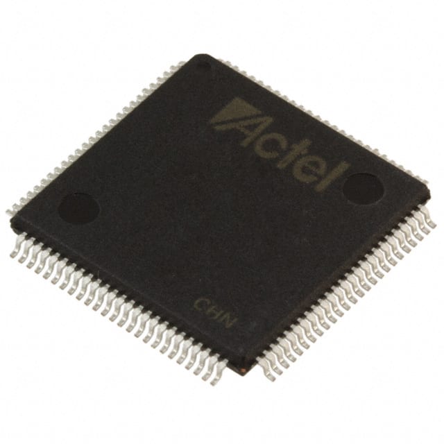
A54SX32A-2TQG100I
Product Overview
Category
The A54SX32A-2TQG100I belongs to the category of Field Programmable Gate Arrays (FPGAs).
Use
FPGAs are integrated circuits that can be programmed and reprogrammed to perform various digital functions. The A54SX32A-2TQG100I is specifically designed for applications requiring high-performance logic integration.
Characteristics
- High-performance logic integration
- Programmable and reprogrammable functionality
- Flexible and customizable design options
Package
The A54SX32A-2TQG100I comes in a compact package, which ensures easy installation and integration into electronic systems.
Essence
The essence of the A54SX32A-2TQG100I lies in its ability to provide a versatile and efficient solution for complex digital circuit designs.
Packaging/Quantity
The A54SX32A-2TQG100I is typically packaged individually and is available in varying quantities depending on the specific requirements of the user.
Specifications
- Model: A54SX32A-2TQG100I
- Logic Elements: 54,000
- Maximum Frequency: 250 MHz
- I/O Pins: 100
- Operating Voltage: 3.3V
- Package Type: TQG100I
Detailed Pin Configuration
The A54SX32A-2TQG100I has a total of 100 I/O pins, each serving a specific purpose in the overall functionality of the FPGA. The pin configuration is as follows:
(Pin Number) - (Pin Name) 1 - VCCIO 2 - GND 3 - IO0 4 - IO1 5 - IO2 ... 100 - IO99
Functional Features
- High-performance logic integration allows for complex digital circuit designs.
- Programmable and reprogrammable functionality enables customization and flexibility.
- Wide range of I/O pins facilitates connectivity with external devices.
- Low power consumption ensures energy efficiency.
Advantages
- Versatile and customizable design options.
- Faster time-to-market due to programmable nature.
- Reduced development costs compared to custom ASICs.
- Ability to adapt to changing requirements through reprogramming.
Disadvantages
- Higher cost compared to traditional fixed-function integrated circuits.
- Limited resources and capacity compared to application-specific solutions.
- Steeper learning curve for programming and utilizing the FPGA's full potential.
Working Principles
The A54SX32A-2TQG100I operates based on the principles of configurable logic blocks (CLBs) and interconnect resources. The CLBs consist of look-up tables, flip-flops, and other components that can be programmed to perform specific logic functions. The interconnect resources allow for the routing of signals between different CLBs, enabling the creation of complex digital circuits.
Detailed Application Field Plans
The A54SX32A-2TQG100I finds applications in various fields, including:
- Telecommunications: Used in network routers, switches, and base stations for high-speed data processing.
- Industrial Automation: Employed in control systems, robotics, and machine vision applications.
- Aerospace and Defense: Utilized in radar systems, avionics, and secure communication equipment.
- Medical Devices: Integrated into medical imaging systems, patient monitoring devices, and laboratory equipment.
- Automotive: Applied in advanced driver-assistance systems (ADAS), infotainment systems, and engine control units.
Detailed and Complete Alternative Models
- A54SX16A-2TQG100I: Similar to A54SX32A-2TQG100I but with 16,000 logic elements.
- A54SX64A-2TQG100I: Similar to A54SX32A-2TQG100I but with 64,000 logic elements.
- A54SX128A-2TQG100I: Similar to A54SX32A-2TQG100I but with 128,000 logic elements.
These alternative models offer varying levels of logic integration to cater to different project requirements.
In conclusion, the A54SX32A-2TQG100I is a high-performance FPGA that provides versatile and customizable solutions for complex digital circuit designs. Its programmable nature, wide range of I/O pins, and flexible design options make it suitable for various applications in telecommunications, industrial automation, aerospace, medical devices, and automotive industries. While it offers advantages such as faster time-to-market and adaptability, it also has limitations in terms of cost and capacity compared to application-specific solutions.
10个与A54SX32A-2TQG100I在技术解决方案中的应用相关的常见问题及解答
Sure! Here are 10 common questions and answers related to the application of A54SX32A-2TQG100I in technical solutions:
Question: What is the A54SX32A-2TQG100I?
Answer: The A54SX32A-2TQG100I is a specific model of field-programmable gate array (FPGA) manufactured by Microsemi.Question: What are the key features of the A54SX32A-2TQG100I?
Answer: The A54SX32A-2TQG100I offers 32,000 logic elements, 1,152 Kbits of embedded memory, and various I/O options, making it suitable for complex digital designs.Question: In what applications can the A54SX32A-2TQG100I be used?
Answer: The A54SX32A-2TQG100I can be used in a wide range of applications, including telecommunications, industrial automation, aerospace, and defense.Question: How does the A54SX32A-2TQG100I differ from other FPGAs?
Answer: The A54SX32A-2TQG100I stands out due to its high-performance architecture, low power consumption, and extensive I/O capabilities.Question: Can the A54SX32A-2TQG100I be reprogrammed after deployment?
Answer: Yes, the A54SX32A-2TQG100I is a field-programmable device, allowing for easy reconfiguration and updates to the design.Question: What development tools are available for programming the A54SX32A-2TQG100I?
Answer: Microsemi provides Libero SoC Design Suite, which includes a comprehensive set of tools for designing, simulating, and programming the A54SX32A-2TQG100I.Question: Can the A54SX32A-2TQG100I interface with other components or devices?
Answer: Yes, the A54SX32A-2TQG100I supports various standard interfaces such as UART, SPI, I2C, and Ethernet, enabling seamless integration with other components.Question: What are the power requirements for the A54SX32A-2TQG100I?
Answer: The A54SX32A-2TQG100I operates at a voltage range of 1.71V to 1.89V, with typical power consumption varying based on the design and usage.Question: Are there any limitations or considerations when using the A54SX32A-2TQG100I?
Answer: It is important to consider factors like thermal management, signal integrity, and power supply stability when designing with the A54SX32A-2TQG100I.Question: Where can I find additional resources and support for the A54SX32A-2TQG100I?
Answer: Microsemi's website provides datasheets, application notes, user guides, and technical support to assist with the implementation of the A54SX32A-2TQG100I in your technical solutions.
Please note that the answers provided here are general and may vary depending on specific requirements and use cases.