

A54SX32A-FFG256
Product Overview
Category
The A54SX32A-FFG256 belongs to the category of Field Programmable Gate Arrays (FPGAs).
Use
FPGAs are integrated circuits that can be programmed and reprogrammed to perform various digital functions. The A54SX32A-FFG256 is specifically designed for applications requiring high-performance and flexibility in digital logic design.
Characteristics
- High-performance FPGA with 54,000 system gates
- 32,768 logic cells
- Fast propagation delay for efficient operation
- Low power consumption
- Flexible configuration options
Package
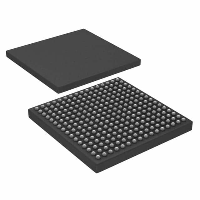
The A54SX32A-FFG256 comes in a Fine-Pitch Ball Grid Array (FBGA) package.
Essence
The essence of the A54SX32A-FFG256 lies in its ability to provide a customizable and reconfigurable digital logic solution for a wide range of applications.
Packaging/Quantity
The A54SX32A-FFG256 is typically packaged individually and is available in various quantities depending on the customer's requirements.
Specifications
- System Gates: 54,000
- Logic Cells: 32,768
- Operating Voltage: 1.8V
- Maximum Frequency: 250 MHz
- I/O Pins: 256
- Embedded Memory: 2,048 Kbits
- Configuration Memory: 4,096 Kbits
- Package Type: FBGA
- Package Pins: 256
- Temperature Range: -40°C to +85°C
Detailed Pin Configuration
The A54SX32A-FFG256 has a total of 256 I/O pins. These pins are used for input/output connections and can be configured to perform various functions based on the user's requirements. The pin configuration diagram provides detailed information about the assignment and functionality of each pin.
Functional Features
- High-performance digital logic processing
- Reconfigurable architecture for flexibility
- Support for various communication protocols
- On-chip memory for efficient data storage
- Built-in clock management resources
- Dedicated hardware multipliers for fast arithmetic operations
Advantages and Disadvantages
Advantages
- Customizable and reprogrammable design
- High-performance operation
- Low power consumption
- Wide range of I/O options
- Suitable for complex digital designs
Disadvantages
- Steep learning curve for programming and configuration
- Limited availability of alternative models with similar specifications
- Higher cost compared to fixed-function integrated circuits
Working Principles
The A54SX32A-FFG256 works based on the principles of digital logic design. It consists of a matrix of configurable logic blocks interconnected through programmable routing resources. The user can program the FPGA using Hardware Description Languages (HDLs) such as VHDL or Verilog to define the desired digital circuit functionality. The programmed configuration is then loaded into the FPGA's internal memory, allowing it to perform the specified operations.
Detailed Application Field Plans
The A54SX32A-FFG256 finds applications in various fields that require high-performance digital logic processing. Some of the potential application areas include:
- Telecommunications: Used in base stations, network routers, and switches for signal processing and protocol handling.
- Industrial Automation: Employed in control systems, robotics, and machine vision applications for real-time data processing and control.
- Aerospace and Defense: Utilized in radar systems, avionics, and military-grade communication equipment for high-speed data processing and encryption.
- Medical Devices: Integrated into medical imaging systems, patient monitoring devices, and diagnostic equipment for advanced signal processing and analysis.
- Automotive Electronics: Incorporated in advanced driver assistance systems (ADAS), infotainment systems, and engine control units (ECUs) for efficient data processing and control.
Detailed and Complete Alternative Models
While the A54SX32A-FFG256 offers a unique combination of features and specifications, there are alternative FPGA models available in the market that cater to similar requirements. Some notable alternatives include:
- Xilinx Spartan-6 XC6SLX45: Offers comparable logic capacity and performance with a different pin configuration.
- Intel Cyclone IV EP4CE115: Provides similar functionality and flexibility with a larger number of I/O pins.
- Lattice ECP5-85: Offers enhanced power efficiency and lower cost compared to the A54SX32A-FFG256.
These alternative models can be considered based on specific project requirements and design constraints.
In conclusion, the A54SX32A-FFG256 is a high-performance FPGA that provides flexibility and customization options for digital logic design. Its characteristics, pin configuration, functional features, advantages, and disadvantages make it suitable for various application fields. While it may have some limitations, alternative models exist to address specific needs.
10个与A54SX32A-FFG256在技术解决方案中的应用相关的常见问题及解答
Sure! Here are 10 common questions and answers related to the application of A54SX32A-FFG256 in technical solutions:
Q: What is the A54SX32A-FFG256? A: The A54SX32A-FFG256 is a specific model of field-programmable gate array (FPGA) manufactured by Microsemi.
Q: What are the key features of the A54SX32A-FFG256? A: The A54SX32A-FFG256 offers 54,000 logic cells, 32,768 flip-flops, and 256-ball fine pitch grid (FFG) packaging.
Q: What are the typical applications of the A54SX32A-FFG256? A: The A54SX32A-FFG256 is commonly used in various technical solutions such as telecommunications, industrial automation, aerospace, and defense systems.
Q: How can I program the A54SX32A-FFG256? A: The A54SX32A-FFG256 can be programmed using hardware description languages (HDLs) like VHDL or Verilog, along with appropriate development tools provided by Microsemi.
Q: Can the A54SX32A-FFG256 be reprogrammed after deployment? A: Yes, the A54SX32A-FFG256 is a field-programmable device, which means it can be reprogrammed even after it has been deployed in a system.
Q: What are the power requirements for the A54SX32A-FFG256? A: The power requirements vary depending on the specific implementation, but typically the A54SX32A-FFG256 operates at a voltage range of 1.2V to 3.3V.
Q: Can the A54SX32A-FFG256 interface with other components or devices? A: Yes, the A54SX32A-FFG256 supports various communication protocols and can interface with other components or devices using standard interfaces like SPI, I2C, UART, etc.
Q: What kind of performance can I expect from the A54SX32A-FFG256? A: The performance of the A54SX32A-FFG256 depends on the specific design and implementation, but it offers high-speed operation and low power consumption.
Q: Are there any development kits available for the A54SX32A-FFG256? A: Yes, Microsemi provides development kits and evaluation boards specifically designed for the A54SX32A-FFG256, which include necessary software and documentation.
Q: Where can I find technical support or documentation for the A54SX32A-FFG256? A: Microsemi's website provides technical support, documentation, datasheets, application notes, and user guides for the A54SX32A-FFG256. Additionally, their customer support team can assist with any specific queries or issues.